 teardownit
Have you ever made a processor? I did. Took me just 12 microchips and a clock generator.
The processor can execute several commands, and programs can be written for it. The program code and input data are entered using micro switches, and the state of the output register is displayed by four LEDs, according to the number of bits.
At first glance, even this circuitry may seem very complex. Still, it consists of simple modules interconnected by data and control buses. Understanding each module's operation and interactions is relatively easy.

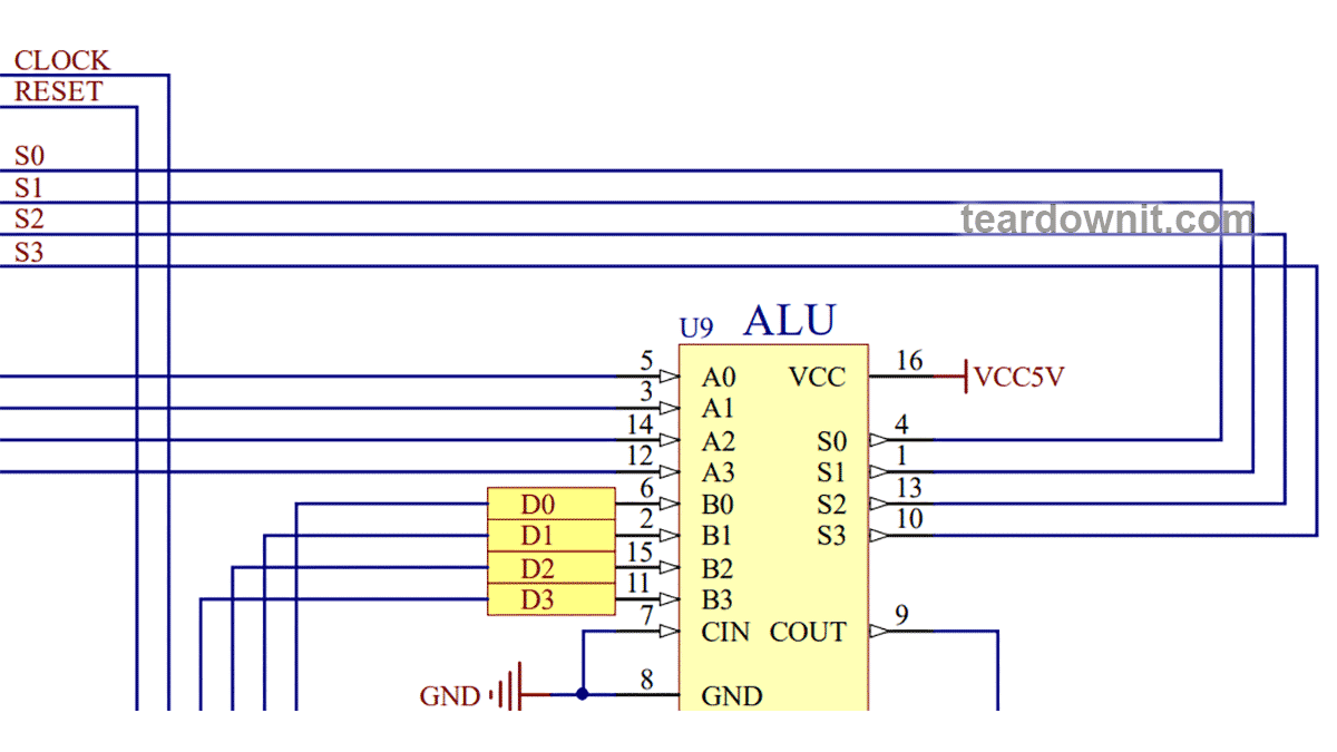
The primary function of a processor is to perform arithmetic and logical calculations. Therefore, our processor is naturally built around an arithmetic-logical unit (ALU).
As an ALU, we will use a full four-bit binary adder SN74HC283N. This chip is asynchronous; it adds two four-bit numbers and outputs a five-bit number (a four-bit number and a carry flag if there is an overflow).
 If you are unfamiliar with the binary numeral system, it's high time to learn it. It is precisely the same as the decimal we're used to; its base number is 2 instead of 10.
0000b = 0,
0001b = 1,
0010b = 2,
0011b = 3,
and so on until
1111b = 15.
If one adds 15 to 15, the resulting number is 30. The corresponding binary number is 11110b. That is 14 plus 16, or 1110b plus 10000b.
In other words, the carry flag here means the number 16, 2 to the fifth power. The SN74HC283N adder considers the presence of a carry flag at the input and outputs a carry flag to the output, which is why it is called a full adder.
So, we have a microchip with two inputs for four-bit binary numbers: A3..A0 and B3..B0.
Why does binary digit numbering start with zero? The digit's index is the power to the base; in our case, the base is 2.
0100b = 4 - 2 to the second power.
1000b = 8 - 2 to the third power.
1001b equals 2 to the third power plus two to the zero power, 8 + 1 = 9.
Any number to the zero power is equal to 1.
The microchip has a four-digit sum output S0..S3 and a carry flag output. It also has overflow input, but we won't use it, so we'll simply ground it. Thus, this input will always be a logical zero.
What can we do with the adder?
We can add two binary numbers and receive their sum.
We have a carry flag that indicates whether the adder has overflowed.
We can add a binary number to 0 by entering 0000b (simply four 0 bits) into one of the inputs. The output will be the same number. You'll see in a moment how this is useful.
So, we've already got ourselves an ALU—not that capable, but enough for us to use. Next, the processor needs registers.
Registers are internal memory cells of the processor meant for direct access. From these exact registers, four-bit numbers arrive at the inputs of the ALU, and the resulting sum is written to them.
The register is based on a synchronous latch. Our asynchronous adder does not save data; its output momentarily pulls its pins low or high, corresponding to the input values.
(To be more precise, it happens almost instantly, but the performance of the SN74HC283N chip is so much greater than the clock frequency of our processor that we can ignore this "almost" part.)
Unlike the asynchronous adder, our synchronous flip-flop changes the state of its outputs only when it receives a clock pulse and is subject to "enable" signals at its control inputs. It will keep its state until the signals at the control inputs are permissive and a new clock pulse arrives.
We use a total of four identical 4-bit SN74HC161N registers in our processor. Strictly speaking, they are not just registers but much more sophisticated multifunctional chips—synchronous binary counters.
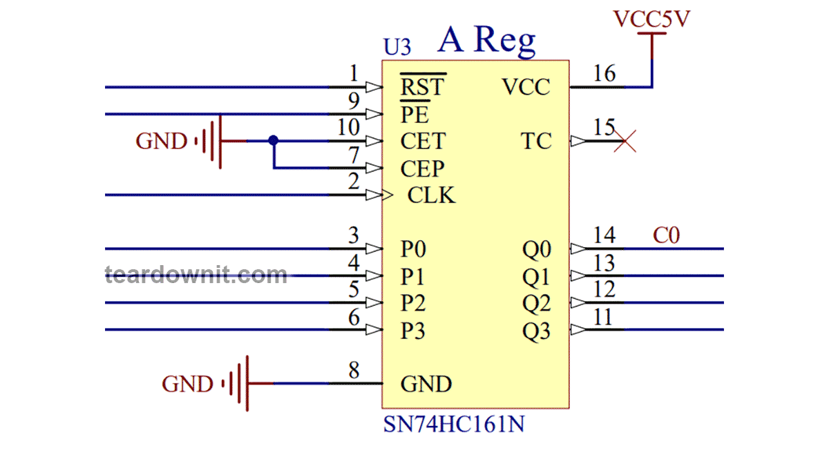 The SN74HC161N chip has a 4-bit input P0..P3 and a 4-bit output Q0..Q3, a carry flag output, a CLK clock input, and four control inputs.
The inverting asynchronous reset input ¬RST sets all 4 latches to zero whenever this input is driven low, regardless of the state of all other inputs.
A low level on the inverting parallel enables input ¬PE allows writing to register Q0..Q3 of data directly from input P0..P3. This will occur on the positive-going edge of the clock.
Parallel enable input is crucial for CPU design. This input allows us to connect all four registers' data inputs P0..P3.
This creates a parallel bus, and the data from it will be read and then written to Q0..Q3 output of the register with ¬PE input set low on the positive-going edge of the clock.
It is possible to set ¬PE input low for multiple registers at once. But we do not need to do it for our processor since it is supposed to output the result of any one of the four available commands to its dedicated corresponding register. We'll elaborate on it later in the text.
The data bus is marked as S0..S3 in the large diagram. The data goes there directly from the output of our ALU, the binary adder.
 In addition to the data bus, our processor will have a reset line and a clock line. In other words, we'll connect the reset and clock inputs of all synchronous data-storing chips together.
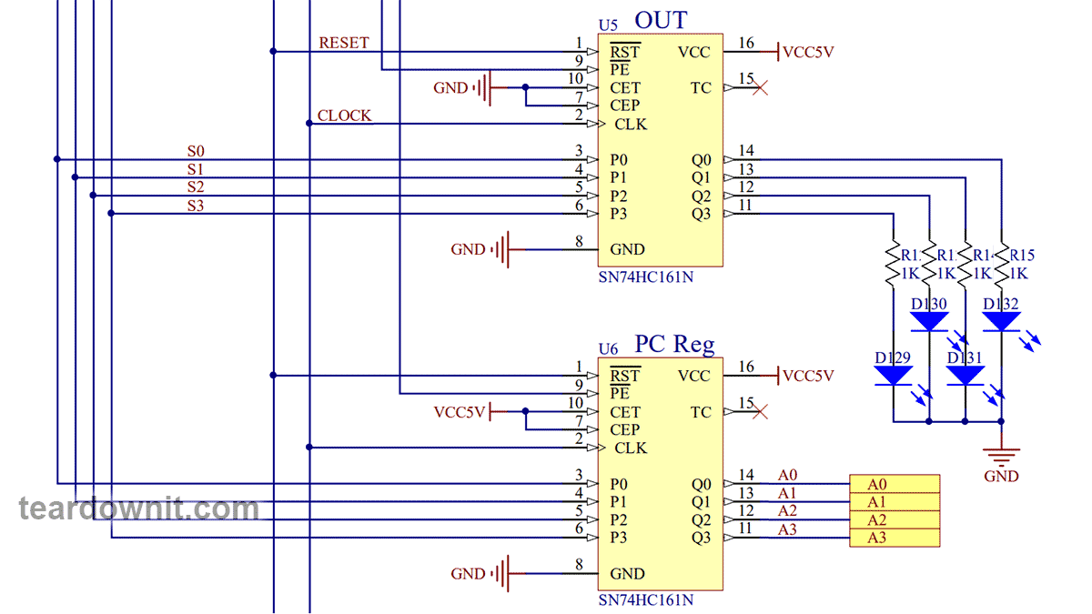 Four LEDs are connected to the OUT Q0..Q3 register output, so we can see the binary number stored in this register.
In addition to reset and clock inputs, the SN74HC161N chip has count-enabled inputs CET and CEP. Both of these inputs must be high for the number at the output Q0..Q3 to increment at each positive edge of the clock pulse.
The two general-purpose registers, A and B, as well as the data output register OUT, have their CET and CEP inputs connected to the ground. Thus, counting is disabled, and the chip operates only as a latch register.
The program counter PC register connects these pins to the positive power terminal. Thus, the contents of this register will increase by 1 with each clock pulse while the ¬PE input is high.
If the ¬PE input is driven low, the program counter value will not increase by 1 in this cycle, and the PC register will store the number from the data bus instead.
This is useful for jump operators. After all, the program counter determines the address in program memory for the processor to execute the command in a given cycle. Here is the diagram of the program memory module.
The output of the PC register is the address bus A0..A3. It is 4-bit and thus can address 16 program memory locations.
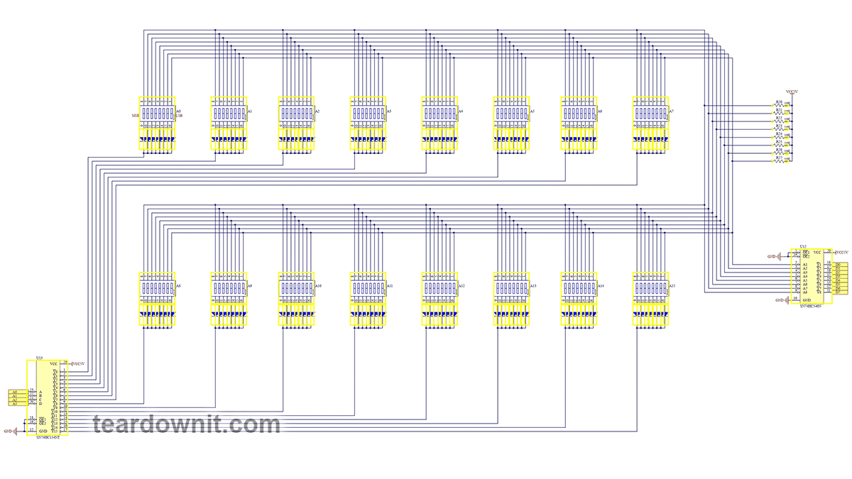
The program memory controller is the SN74HC154N decoder. Fifteen of its sixteen outputs ¬Y0..¬Y15 are pulled high. One of the outputs is low, corresponding to the binary number A0..A3. This determines which program memory cell is read in a given cycle.
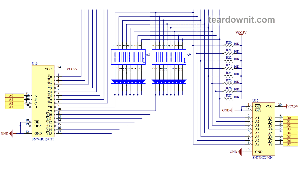 The program memory cell is an 8-bit microswitch. Bits with switch contacts closed are pulled low through diodes. And those with contacts open are pulled high through 10 kOhm resistors.
SN74HC540N is an inverting buffer. As a result, D0..D7 will have logical ones where the microswitch contacts are closed and logical zeros where they are open.
The LSBits D0..D3 store the value, the second binary operand for our ALU adder.
The MSBits D4..D7 contain the operation code, the actual command for the processor. The first operand for the ALU is selected by this very command.
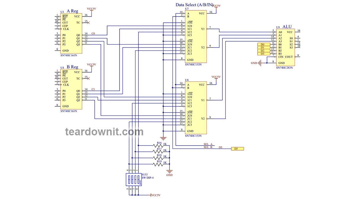
If the SN74HC154N decoder is a 4 by 16 demultiplexer, then the SN74HC153N is, on the contrary, a dual 4 by 1 multiplexer. We need two of these dual multiplexers to load a single 4-bit operand into the ALU.
If A = 0, B = 0, the ALU will receive data from register A. If A = 1, B = 0, then the operand will be the contents of register B, and if A = 1, B = 1, then logical zeros.
Finally, when A = 0, B = 1, the operand is taken from the 4-bit microswitch, the input register.
Where do these SEL A and SEL B signals come from? As for SEL B, it's simply the fifth digit from the program memory cell, D5. D4, D6, and D7 proceed to the program decoder.

This decoder is put together based on two logical gate ICs. SN74HC10N is a dual 3NAND gate, and SN74HC32N is a quad 2OR gate.
The control line of the SEL A multiplexers is connected to the output of the OR gate. At the same time, its inputs receive bits D4 and D7 of program memory. If at least one or both are equal to one, then SEL A will be set high; otherwise, the output level will be low.
So, we can indicate where the operand for the ALU comes from using bits D4, D5, and D7. We must also let the processor know which register to store the additional result.
A low level on line ¬LOAD0 selects register A. ¬LOAD0 = D6 | D7, meaning register A will be selected for the result if both D6 and D7 are zeros.
We can already start understanding what some of the opcodes will do.
0000 - ADD A, Im. SELA = 0, SELB = 0. The contents of register A plus the immediate value from D3..D0 is loaded into register A.
0001 - MOV A,B if Im = 0, or A = B + Im. Loading the contents of B into A with the ability to add immediate value.
0010 - IN A with Im = 0 or A = IN + Im. Entering a number from the microswitches into register A, again with the ability to add a direct value. Any instruction has this opportunity since our ALU is an adder.
0011 - MOV A, Im. Loading the immediate value into register A. It is added to zero since SELA = 1 and SELB = 1.
A low level on line ¬LOAD1 selects register B for the result of the operation. ¬LOAD1 = ¬D6 | D7, meaning that to select register B, D6 must be high and D7 must be low. Therefore, the following four opcodes are obtained.
0100 - MOV B, A with Im = 0 or B = A + Im.
0101 - ADD B, Im.
0110 - IN B or B = IN + Im.
0111 - MOV B, Im.
A low level on the ¬LOAD2 line uploads the result of the operation to the OUT register, i.e., to the LEDs. ¬LOAD2 = ¬(¬D6 & D7) D6 should be 1, and D7 should be 0.
1000 - OUT B at Im = 0 or OUT = A + Im.
1001 is the same as 1000 because SEL_A = D4 | D7.
1010 - OUT Im.
1011 is the same as 1010 because SEL_A = D4 | D7.
Finally, selecting the PC register (the operators of moving the program counter pointer to the desired program memory address) corresponds to the bit values D6 = 1 and D7 = 1.
It gets somewhat more complicated from here. Let's take another look at the command decoder scheme.
As you can see, there is also a synchronous D-trigger U1B of the SN74Н74N chip in the processor schematics. I absolutely love this chip; it allows one to do many interesting and useful things.
In this case, the trigger remembers whether the adder overflowed in the previous cycle. Just like our four counter registers, it is clocked by a common CLOCK line and reset by a common RESET line.
¬LOAD3 = ¬(D6 & D7 & (¬C | D4))
This means that when D6 = 1 and D7 = 1, writing to the PC register will occur only if one of the two (or both) additional conditions are met.
If D4 is low, the transition will only occur if there is no adder overflow in the previous cycle. This way, we have a conditional transition.
1100 - JZ B at Im = 0 or JZ (B + Im).
1110 - JZ Im.
If D4 is high, an unconditional jump occurs.
1101 - JMP B with Im = 0 or JMP (B + Im).
1111 - JMP Im.
So, we've looked through all 16 possible commands on our tiny processor and are ready to test them out. But the processor still needs a frequency generator.
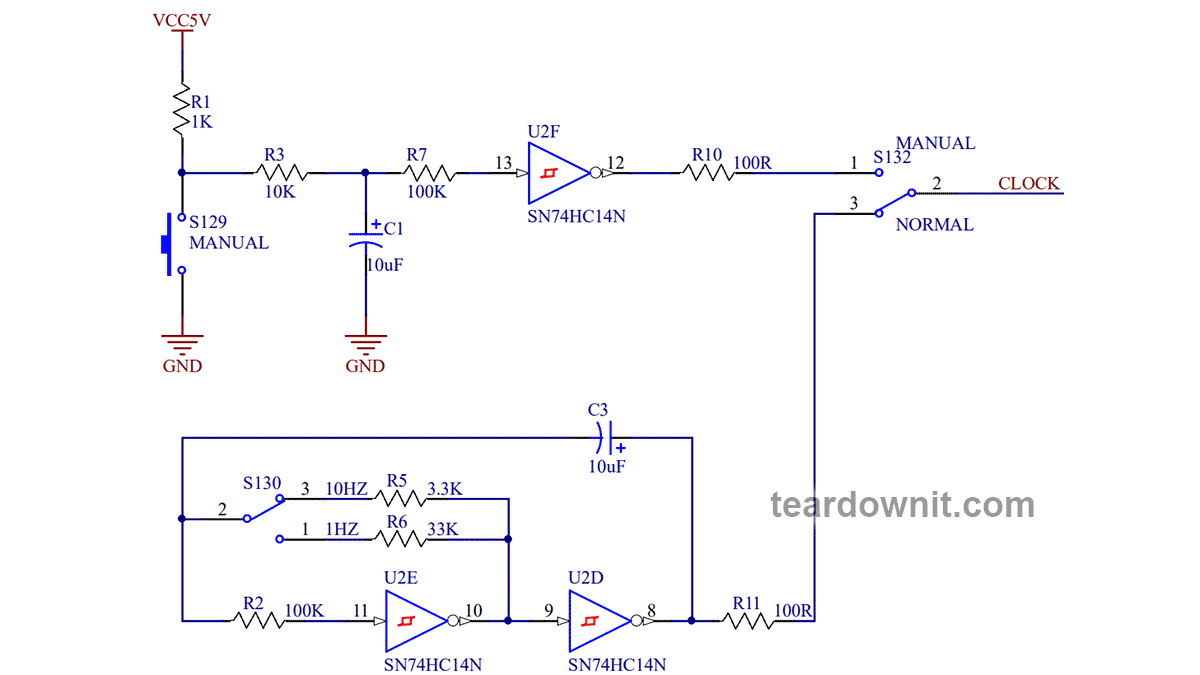
Our clock is straightforward. It is made from two inverters of the SN74HC14N microchip. The S130 switch allows one to select the clock frequency: 1 clock cycle or 10 clock cycles per second.
Using the S132 switch, one can toggle between clock-driven and step-by-step execution of the program with a push of the S129 button, which is also equipped with an inverting buffer thanks to the SN74HC14N chip.
Now, let's try to write a program for our small processor.
0000 OUT B 1001 0000; display the contents of register B with the LEDs
0001 ADD B, 1 0101 0001; add 1 to B
0010 JZ 0 1110 0000; if there was no overflow, go to address 0
0011 IN B 0110 0000; read the number from the micro switch
0100 OUT B, 1 1001 0001; return this number + 1
0101 JZ 11b 1110 0011; if there was no overflow, go to address 11b
0110 MOV A, 0 0011 0000; so that the count starts from zero once again
0111 MOV B, A 0100 0000
1000 JMP 0 1111 0000; unconditional jump to address 0
This program will output numbers from 0000 to 1111 to the LEDs and then output the number entered by the microswitches plus 1 until 1111 is reached. Then, the adder will overflow, and the program counter will return to the beginning of the program.
On line 0110, we could just write MOV B, 0, which means register A wouldn't be used in the program. And we want all our registers to be used.
Suppose one does not clear the contents of register B before jumping to the beginning. In that case, it will still contain 1111 and immediately cause an overflow in line 0001. As an outcome, instead of binary numbers 0000 through 1111, we will see LEDs switching from 1111 to 0000 and back.
As you can clearly see, the program works exactly as intended. This means that we have not made any mistakes along the way.
"TD4 CPU" is an open-source project; it can be downloaded from https://github.com/wuxx/TD4-4BIT-CPU.
Discussions
Become a Hackaday.io Member
Create an account to leave a comment. Already have an account? Log In.