 Ken Yap
Update 2020-01-15: Got email from them saying they have merged with Ocean Smile (who thinks up of these names?) with a new site. As far as I can tell the pricing structure is unchanged and my old account works so my next 4 5-board orders are still $2.
The story is finished: LocoPCB was offering 5 100x100 mm boards for $2 + shipping. Gerber files were uploaded and after one to and fro with the customer rep, it was sent to processing and then manufacture. I misunderstood the difference between those two stages, read the Order Status section below. It was shipped. I received the board just before the new year and I reviewed the quality below as well as the V-cut feature.
Ocean Smile PCB
I saw ads from LocoPCBOcean Smile on PCBShopper many times and when I saw that they were offering 5 100x100 mm boards for $2 + shipping I decided to give them a try because they offered V-cut panelisation for free. Their office is in Shenzhen but the factory is in inland Guangzhou.
The loco referred to locomotive as you can see from their logo. I wonder how people react to the name in Spanish speaking countries. I suppose it's still publicity.
Board
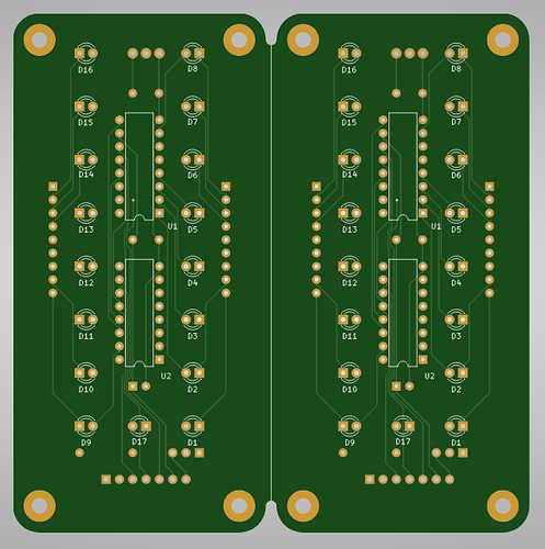
The board is actually under 100x48 mm so I made 2 panels per board by using the Append PCB operation in pcbnew, then adjusted the outline (Edge Cut). V-cuts must be from edge to edge. Both top and bottom of the PCB are scored, leaving about 1/3 FR4 material. Should be interesting to see how hard it is to separate the halves compared to breaktabs and mousebites.
To ask for V-cuts in the form you tick the Customer Panel option, and the V-cut should be an edge to edge line in the Edge Cuts layer. This confuses the 3D viewer once added, as the outline is no longer a closed polygon, so you will not be able to view the board outline there, though the rest can be viewed. One complication is that I wanted to preserve the rounded corners so I had to leave 2 mm bays so that the router could cut that. Here's what the board looks like:
Ordering
While consulting their support pages for requirements I found that the images wouldn't display in Chrome. The reason is that the page are served by https but the images are served by http. Chrome considers this insecure. Firefox will display it with a warning in the location bar. I sent a bug report to their IT department. (2020-01-01: Their order pages have been under refurbishment since mid-December, hopefully fixing the http/https problem.)
Like other fabs you fill in the form and upload the Gerber archive. You have to pay (Paypal or Visa) before it is checked.
I had noted that unlike many other fabs they want PTH (Plated Through Hole) and NPTH (Non-PTH) in one file. This is an output option in Kicad/pcbnew. But I had failed to note that Include Extended (X2) Attributes should not be selected. And Protel file extensions of course. Must be older software that they are using. As a result, the customer rep asked me to resubmit. The redone archive worked. So to summarise:
- Protel file extensions
- Enable PTH and MPTH in a single file
- Disable Include Extended (X2) Attributes
Order tracking
Each account has a page for tracking orders, Naturally I had only one order in the table. The usual details are shown. Some of the GUI elements like View Detail and Invoice can be clicked on, some show popup windows when moused over, such as Ship To. The Tracking element becomes live when tracking information is available. But since it's obtained from the carrier, some lines are in Chinese and you will need a translator if you don't read Chinese and are really interested in where your package is.
Order status
First the status showed processing. I thought this meant it was being made, but it turns out that this is probably just the stage where they prepare the design material such as files to drive the machinery. It stayed in this stage for 3 days.
After that it went into manufacturing. This should be where they actually make the board, i.e. the chemical and mechanical processes. It spent 2 days here, in line with their advertised 48 hours.
After that the status changed to ready to ship, and then changed to shipped.
This status line was the only progress indicator I saw, where some other fabs actually show you the part of the process it is going through. Spending 3 days in processing isn't what I expected 48 hour turnaround to mean. I think this is because for cheap orders there are engineers who try to fit the order on the unused parts of the large board containing many other, probably higher value orders. Well, I can't really complain for the $2 price and really I'm not in a hurry.
I chose the cheapest shipping option E-packet so it will be at least 2 or 3 weeks before it gets here.
Board evaluation
I received the boards just before the new year about 3 weeks after dispatch. The first surprise was that when I took the boards out of the customary shrink wrap plastic packaging there didn't seem to be any V-cut on the board. There was a line but I thought that was the silk screen line I had put there. Oh no I thought, they must not have acted on the line I put in the edge cuts layer as well as the note I added to the order. Now I'll have to cut the board with a Dremel and report this to Hackaday.
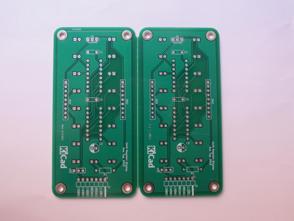
But when I tried to flex the board a little I found that it did bend a bit more than expected of FR4. The V-cut was there, just narrower that I had expected. If you look at a cross section you'd probably find a 15° V rather than the 30° or 45° I was expecting. Bending the board broke through the middle third of the FR4 at the V in a gradual and satisfying fashion, unlike the sudden snap when you bend a board with mouse bites.
So the V-cut worked as expected, from the discussion I had on the Kicad forum. Because the V groove was not as wide as I had expected there is a wider ledge from the rounded corner to the V edge, which you can see here:
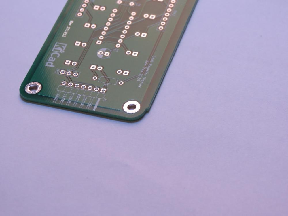
That's the price for wanting rounded corners. To avoid this one would have to make 2 V-cuts separated by a rail of at least 5 mm but this means 5 mm is not available for the panels.
A couple of other features to note on the penultimate photo: 1. There is a small job number placed by LocoPCB at the top of the board. 2. The letters for Rev 201912 to the left of the Kicad logo are actually silver, in solder. This is a trick I learnt on the Kicad forums, you put text on the solder mask, and because the mask layer contains areas where the mask is removed, any text there will show the underlying area, in this case the copper after HASL (or other) treatment.
I see no problems with the production quality, it's as good as any of the other fabs I've used. Bear in mind this is an undemanding board using THT, but I don't expect problems with SMT footprints. The problem for LocoPCB is that they are up against other fabs offering similar prices, notably JLCPCB, but not charging for V-cuts will be in LocoPCBs favour.
I will review the board operation after I have assembled one for the #An uninnovative linear LED display project. I don't expect any problems.
Discussions
Become a Hackaday.io Member
Create an account to leave a comment. Already have an account? Log In.