 Eric Hertz
Here's the full-schematic, so far:
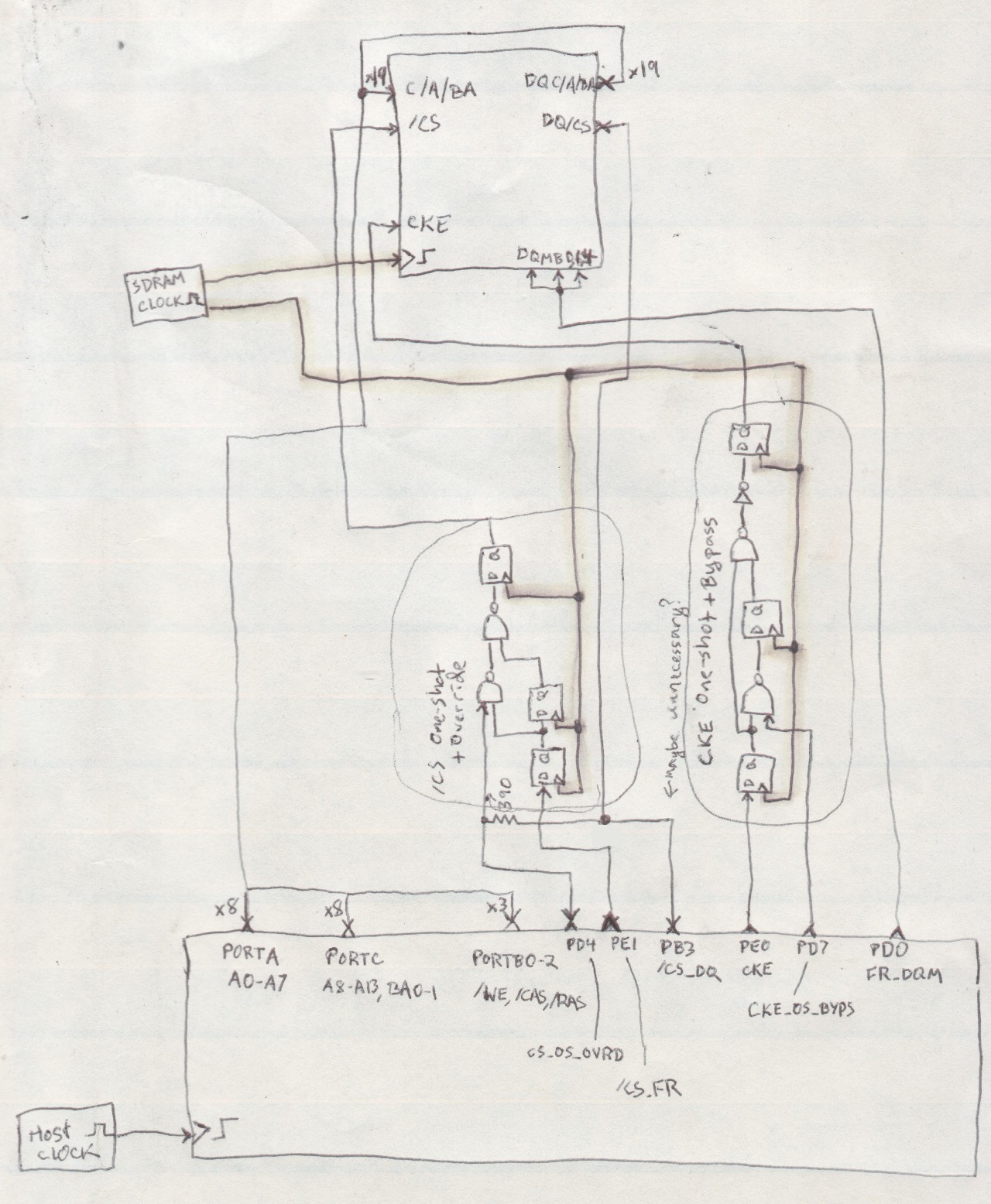
Chip-Select and Clock-Enable need one-shot circuits... Their outputs should strobe for only one SDRAM-Clock cycle, regardless of the Host-Clock (as long as the host's CKE and /CS outputs are >= one SDRAM-Clock-Period). All other signals don't really matter. And, there are times CKE should remain active constantly. /CS should do the same (at times). Thus the Bypass and Override signals.
Those circuits would be a little more intuitive if I hadn't used NAND gates (due to supplies), and hadn't included the Bypass and Override signals. But, actually, the NANDs help to make those override/bypass signals easier. (Originally, on #sdramThing4.5 "Logic Analyzer", I used 7474's which have Set and Clear inputs, those made Bypass/Override pretty easy, but the 74HC74s in my posession are a bit slower than the 74AHC574 I ended up using this time 'round, which doesn't have Set/Clear inputs).
Basically, all those circuits do is look at the "last" value and compare it to the "current" value, if there's an appropriate change (high-to-low for /CS, low-to-high for CKE) then it outputs the appropriate value (low for /CS or high for CKE).
Note that I haven't yet reimplemented the "Side-Kick" half of the SDRAM, which would be the part that samples the logic-analyzer's inputs. That'll add a good 32 data-bits, at least one Chip-Select DQ, and 4 DQM signals... so there's still a bit to be done.
Currently this system uses 16 I/Os for Address/Bank-address and associated DQs, 3 I/Os for directly-fed-back command inputs/DQs (/WE, /CAS, and /RAS). That's 19 directly-fed-back signals (wired directly to DQs).
It's a bit difficult to see the feedback-path between DQ_/CS -> /CS. This travels through the resistor onto the CS_OVERRIDE input (meaning the "host" has to turn that signal to an input/Hi-Z during free-running).
Now that I've drawn the entire schematic, I wonder if the /CS_DQ host-pin (PB3) is necessary... Removal might add a couple "steps" to the timing-diagram, but would save a pin... And, *Maybe* it would be possible to remove the resistor as well(?).
Alternatively (maybe), I drew some timing-diagrams of what'd happen if I use *one* pin for both CKE_OS_BYPASS and /CS_OS_OVERRIDE... It's possible to do-so, but doing-so inverts the /CS signal at certain times, which would add "glitches" during switchover, and also require thinking, in software, that during those times the /CS output from the host is actually active-*high*, whereas at all other times it's active-low.
So, now, contemplating switching-over to a higher-power microcontroller for continued experiments... (I'm running out of memory on my ATmega8515, which is actually kinda strange considering how much I accomplished with the same chip on sT4.5, I think I ended up removing all the serial/stdio stuff from that guy, as well as 'heartbeat' which takes a bit of code-space)...
But, switchover will also aid in development toward the host-independent host-bus interface. Am imagining an interface similar to the 8051's bus-system, with *maybe* an "address" line, or two, that would *not* correspond to an address in the SDRAM, but rather be more like the "Register-Select" pin on a HD44780-based text-LCD. This'd probably be used for selecting whether we're doing reads/writes to control-signals (/CS, CKE, DQM, etc) or to whatever chip-DQ's are selected by those control-signals.
Looking into some various sorts of "hosts", that seems like a reasonable way to go... E.G. the FT2232H happens to have a mode or two like that (which also happen to run at 60MHz!) so connecting this system to a computer of any sort via USB wouldn't be difficult. And, that bus-interface is standardized-enough these days that many other microcontrollers have direct support for it (e.g. the ATmega8515 I'm using has an "External Memory" interface, the PIC32 I plan to move to next has a "Parallel Master Port"...
Only thing is, "strobing" CKE is necessary for reading-back or writing bursts of data, and on the 8051-style bus, I think, strobing like that would correspond more to e.g. the "/WE" or "/RD" signals. And, further, that using a host-interface like that *as designed* would result in the entire timing-transaction (loading the address, strobing ALE, prepping for data, strobing, etc) whereas, again, e.g. during a burst, there's no need for that entire transaction for every data-byte. And, yeah, that sorta stuff adds up... even just adding *one* extra transaction would change a 60MHz bus down to 30MBytes/second... adding *six* would drive that down to 10MB/s, and so-on. And... I've already shown how many transactions are necessary just to set-up a write to a single location, in the free-runner anyhow. (Currently, loading 64MB of free-running data--which looks to correspond to about 2 seconds of sample-time from a logic-analyzer running at 22MS/s--takes over a minute, with my AVR running at 16MHz... That means you've got a "boot time" of over a minute, before data can be sampled! And who knows how long to *read back* 64MB of sample-data! Thankfully that "boot" procedure only has to happen once!)
So... I'm contemplating the best method to wire-up these signals to a bus... Should I have a multiple-byte transaction...? E.G. The first byte selects *which* register to access, then the second byte reads/writes it? Or maybe, more logically, that'd be handled by ALE (which is *not* used on e.g. a text-LCD, and *not* available on things like parallel ports). And those strobes... should they be their own dedicated signals (not compatible with the 8051 bus, requiring dedicated GPIOs) or should they be registered like everything else (and require *two* *full* memory-transactions at 6 or so transactions/bus-cycles apiece to strobe what could've only been *one* bus-cycle). Similarly, should I whittle this down to an 8-bit data-bus, or maybe 16 would be better... For the greatest compatibility, 8, but for speed 16... yahknow. Lots to think about.
Now that I've got the full schematic sitting in front of me (rather than sub-circuits laid out as comments in the code) it's easier to get a higher-level view of the system/IOs.
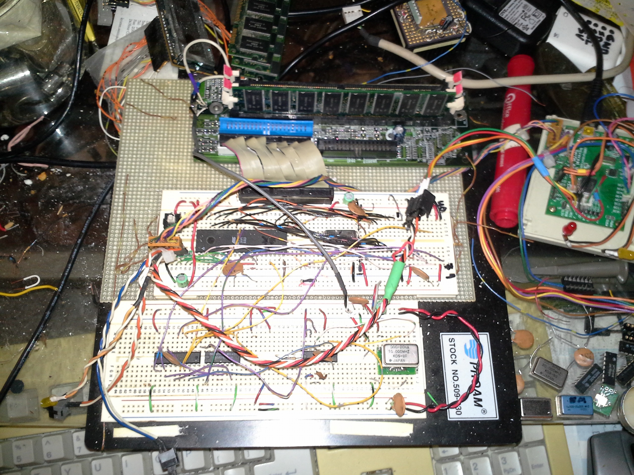
(Ah Hah, I was running the SDRAM at 16MHz, last time...)
So, the Crystal Oscillator is sitting on a breakout-board I made with a CY2305 clock-regenerator... One output goes to the SDRAM, the other goes to the 74AHC574 octal-D-latch. The AVR is running on a separate crystal-oscillator, (currently also 16MHz, though I have been doing lots of experiments verifying functionality at lots of different clock-rates and combinations thereof).
The twisted-cable leading to the circuit on the right is serial output. The other is for programming the AVR... using an FT2232H breakout-board. The heavy gray cable is shielded for the SDRAM-clock.
...And free-running works with three different DIMMs from different manufacturers.
Discussions
Become a Hackaday.io Member
Create an account to leave a comment. Already have an account? Log In.
I can... sort of... understand that. It will make more sense when I look at the timing signals... not important right now.
No chance that a RasPi could be the direct controller? It has a very nice DMA system from what I understand. But no where near enough IO pins without some sort of expansion.
Or what about an FPGA as the controller? One with a core built in? Like the SiLabs PSoC series or TI Tiva?
Are you sure? yes | no
Haha, you really like the Pi/FPGA ideas, huh?
In fun, I'll repeat the Project Description, This is intended to be more of a *peripheral,* than an entire system, It's host-less, as in it "Haz Zero Hozt."
But, that's *exactly* the point, If you want to connect it to an FPGA, a RPi, or even an Arduino, feel free :)
That info you gave regarding FPGA kits in a past log was great, but those, alone, were upwards of $40 and didn't have nearly enough I/O pins, nor exceeded clock-rates of 100MHz, so *directly* connecting an FPGA to the SDRAM (without adding this bus-circuitry) would require even larger/faster FPGAs (most of which, I've seen, are BGA, not particularly "hacker-friendly").
The reason for using discrete logic (latches) and resistors to whittle all these pins down to a bus, rather than going *through* a processor or FPGA is *exactly* what you're getting at...
The 8051-style bus-interface is standard-enough that *a ton* of processors, these days, have *direct*-support for it, *and* via DMA.
I'll need to look into the specs for the RPis to see whether their GPIOs *directly* support it, my guess is *no*. (Which is the ironic, to me, thing about RPis, being that they have a darn-near identical bus onboard going to other chips (like FLASH), just not making those pins accessible).
This page seems to confirm that, and is similar to what I'm doing:
https://www.raspberrypi.org/forums/viewtopic.php?t=59921&p=468410
The Pi GPIOs could certainly be made to work *like* this bus, however... (just as, for this early-early prototype I'm using an AVR's GPIOs).
There, then, might be some debate as to whether interfacing this bus to the Pi's GPIOs and "bit-banging" the (parallel) bus would be any faster than e.g. feeding *this* bus into shift-registers, and using the Pi's SPI peripheral (with DMA) to access the device. Certainly doable, but a step I plan to leave to the implementers.
Note, numbers I've seen put RPi GPIO-toggling at an absolute-maximum of roughly 50MHz, whereas the SPI peripheral can handle clock rates of 250?!MHz. If the latter's true, then SPI+DMA might, indeed, be significantly faster (with a Pi), despite loading the data serially, rather than in parallel. (Whether I'm capable of designing a PCB capable of 250+MHz signalling, and finding appropriate shift-registers, is another thing entirely. An alternative seems to be presented in the link, above).
Still, as far as I'm aware, 64+bit SPI (to handle all the necessary SDRAM pins) isn't a normal thing, so we'd still need to whittle the interface down to a reasonable number.
Further, again, if this was being connected to (many hacker-friendly) FPGAs, or an Arduino, it'd be *much* faster to load that data in parallel. Though, again, I'm assuming that the SDRAM's clock is faster than the host's clock.
At the point of high-pin-count FPGAs, there's really no *need* for sdramThing, just throw a DIMM at your FPGA and drag the SDRAM-interface block to the window to program it to do whatchawant. That's an entirely different project (and surely a great learning-experience for those interested in FPGAs... and get a slightly more sophisticated FPGA, and throw DDR at it!).
Are you sure? yes | no