 Eric Hertz
OK, so I'm not great at linear-algebra after a decade... But I still know how to solve equations for variables. I tried to account for the inequalities, and it got pretty ugly...
( (>=9) - V ) * y <= ( (<=1.5) * V - (<=3) ) * x
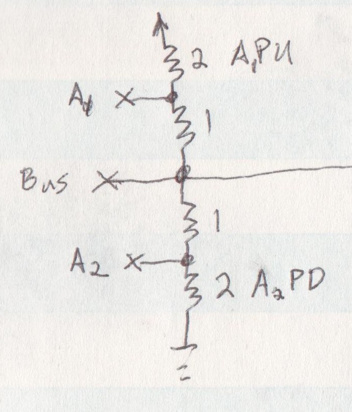
But it doesn't take a whole lot of sophisticated math to solve a voltage-divider equation for a resistance... and, unfortunately, it looks like the idea, from previous logs, of loading "default" values onto the address-inputs via pull-resistors, *while also* tying those address-inputs to the "bus" via nothing but resistors, just isn't possible...
It was *right* on the threshold.
Using 3V for V+, assuming that the "bus" would drive at 0V or 3V, and assuming that VIL-Max = 1V... it actually works-out. Pretty easily, using voltage-divider resistances of, essentially, 1x and 2x, giving 1/3Vin or 2/3Vin, as necessary.
But the reality is, the bus would likely be driving something less than 3V for "high" and something higher than 0V for "low"... And, if I've done my math correctly, it's just *not possible* to find suitable resistances for all the cases. SO CLOSE.
Realistically, it'd probably work with the 1x and 2x resistance-values (using 3V). But it would definitely be out-of-spec.
So, there're a couple options...
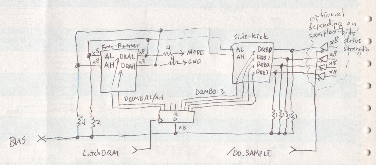
Part of what makes the ADDRESS pins different than the Side-Kick's data-bits is that the address inputs have to be set-up simultaneously (that's two bytes) at least in one case (loading the Mode Register, necessary for initialization).
The Thought was to use Pull-Up/Down resistors to set a default value. That works... What doesn't work is that in order for the Bus to Drive the address-inputs (later down the line) means that it's fighting the pull-resistors... No problem with that. The problem is with the fact that the only way it *can* fight those pull-resistors is *through* other resistors (the ones marked "1"). And, for it to be within-specs while driving the A1 or A2 inputs, it would require *much smaller* resistances than "1"... which means that our "2"s and our "1"s no longer add-up to VIH-Min at A1 and VIL-Max at A2 when the bus is High-Z.
Ooooh Kayyy...
Using that technique, though, I still might be able to get away with removing *one* latch from the original design. Use *one* latch for *one* of the address-bytes, and load the other address-byte onto the bus. Or, that'd be the logical-conclusion. EXCEPT... Remember, this bus is shared not only for address, but *also* for data AND *command* signals.
So... still some thinking to be done.
Here's how I originally saw it... Note that the "Side-Kick"'s 32 bits are connected to the 8bit bus... these should be no trouble, as each byte's "Output-Enable" (and input-enable!) can be individually selected.
...
So, there're several options for address... (Heck, I could add 74x244's between the pull-resistors and the address-lines, not unlike the side-kick)... but if I'm adding chips maybe the most logical is just to add latches between the address signals and the bus. And, if you saw that previous log, you'd've noticed that making use of the Address-lines in the way shown results in quite a bit more software for *each* command making use of an address (Activate Row, Read/Write, Precharge...). Kinda cool that it's possible to do that way, but probably not ideal (and definitely slower).
Still... having a hard time letting go of this one. Wee!
Discussions
Become a Hackaday.io Member
Create an account to leave a comment. Already have an account? Log In.