 Eric Hertz
(UPDATE: 10-19-16 THIS IS WRONG!!!! See the bottom for corrections!)
In #sdramThing4.5 "Logic Analyzer" I used a 74x51 as a multiplexer... Not exactly sure *why* I chose that, over an actual mux-chip... but I did. Maybe I didn't have any 2-in/1-out muxes, or maybe I wanted to have the option to *not* choose either input (then I'd've needed a 3-in/1-out mux, or a 2:1 mux with an enable input).
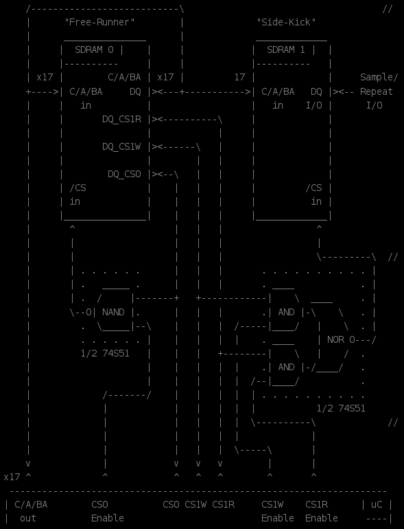 So, on the "Side-Kick" side of things, you see the 1/2 74S51, the '51 has two "and-or-invert" sections like this. The second was turned into a two-input NAND for the "Free-Runner" by tying its other pins low. And, functionally, it basically acts like a MUX (inverting) whose "other" input is tied low.
So, as I understand, And-Or-Inverts are somewhat common because they were used extensively for selecting a memory or I/O device on a bus with several memory or I/O devices. E.G. the memory-device may only use 10 address-bits... Then one AND's input might be connected to A12... And the And-Or-Invert's output might be connected to the device's /Chip-Select, making the device active only when A12 is active (despite the device's only having a 10-bit address bus). (I wrapped my head around it once, now the brain's not functioning in that realm... I'm sure search-fu would return a bit).
And-Or-Inverts can also be used as an inverting-multiplexer... Tie one input of each AND together, one through an inverter... And you have a 2-input/1-output MUX (with an inverting output).
------
For This Project, sdramThingZero, I'm trying to minimize the specialty-parts requirements... So seeing what I can get away with, hopefully using little/nothing more than 74x574 or 74x374 latches and NAND gates (74x00).
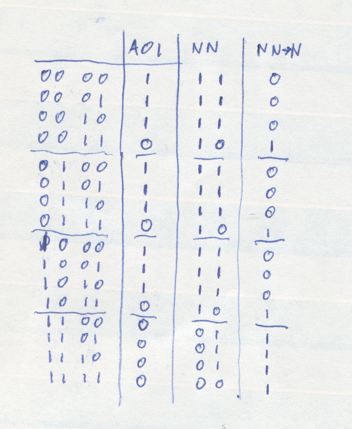
Interestingly, it turns out, And-Or-Invert is *exactly* the same if you replace the ANDs and NOR with NANDs. (ignore the inverters, for now... they're not part of the equivalent And-Or-Invert circuit)
NO NO NO!!! THIS IS WRONG, SEE THE BOTTOM!
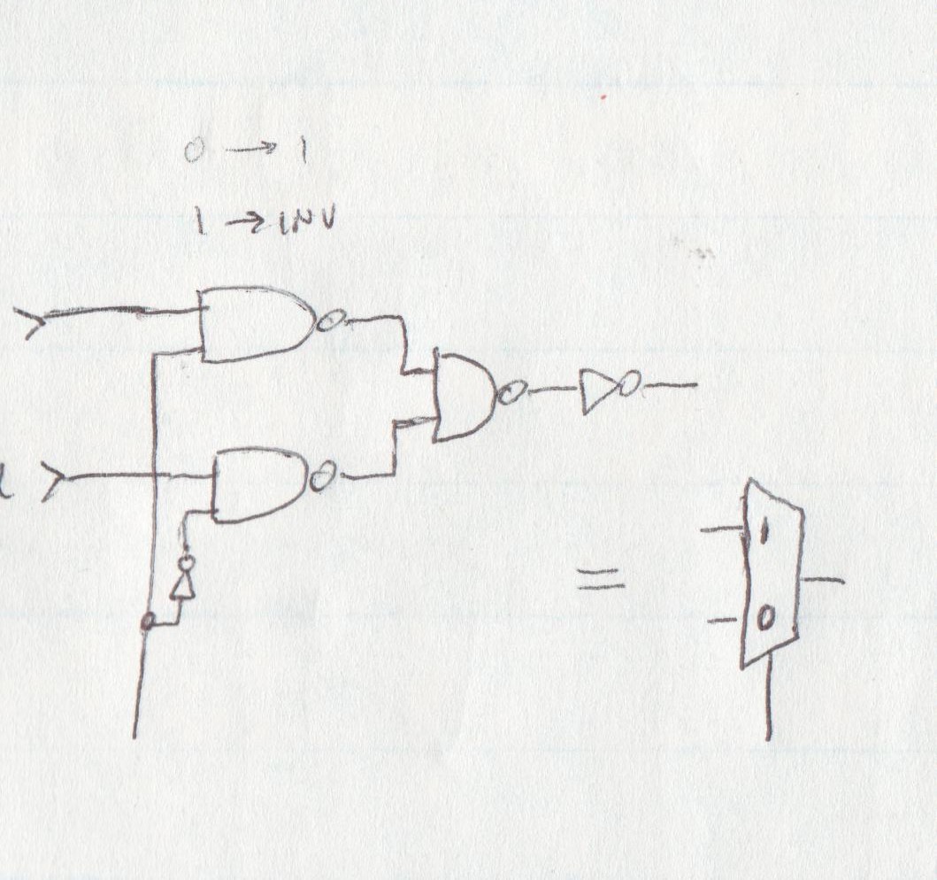
Here I've thrown in an inverter on the two ANDs' inputs, as described earlier, and thrown an inverter on the output to make it a regular-ol' (non-inverting) MUX.
Anyways, I just found it interesting... They *call* them And-Or-Inverts, but they're probably *designed* with NANDs, since, as I recall, NANDs are one of the easiest gates to implement at the transistor-level (more-so than AND). There's a name for that technique of swapping ORs with NANDs by inverting their inputs... I can't recall what it is. The same is used in programming, e.g.
(A && B)
is equivalent to:
!(!A || !B)(Don't quote me on that, that's from memory, and again my brain is not functioning in that logical-realm right now).Anyways, I found it interesting.
---------
THIS PART SHOULD STILL BE ACCURATE-ISH...
Other reasons for trying to stick with e.g. NANDs (and D-Latches) rather than using dedicated (multi-gate) chips...
Well, we're talking about pushing this system up to 133MHz... that's pretty fast for most logic. If not for the logic itself, then consider the delays in wire-lengths, etc. They may not be a *big* deal, yet, but something to consider.
So, here's my rationale... Many/most of the logic used in this system *can* be delayed by several clock-cycles, as long as you *know* how much they're being delayed... and account for it.
There was a time (and maybe it still is?) that gate-delays were actually *intentionally* used... say you have a bunch of data-signals that need to be clocked in to a latch... and all those data-signals switch at the same time as the clock... It was (is?) actually considered somewhat standard-practice to insert a gate between the clock-signal and the clock-input such that the data would be known to be steady before the clock-input gets clocked. Sometimes you'd even see multiple buffers tied in series for exactly that purpose. This was *often* done in the purely trial-and-error realm... One can't *rely* on a chip's propagation-delay to be *exact*, and most chips would specify *maximums* not minimums. (Hey, most people consider it better if their chips run *faster* than spec'd, right?). So, sometimes you'd even see production-boards where a bunch of buffers are tied in series, and a hand-soldered wire is soldered to whichever gate's output gave the appropriate delay. Similar is done in the *really high-speed realm* by e.g. using "snake" traces... increasing the length of the clock's electrical-trace by a bit, compared to the data-signals' trace-lengths. (Though, "snaking" is probably more-often used to *match* trace-lengths).
So, back to our circuit... let's take a look again at that '51 (or the NAND-equivalent)... say one gate-delay is 3/4ths of a clock-width... In most cases it'd probably work OK to insert *one* gate between a signal. But *two* gates would be 3/2's of a clock-width, 1.5 clocks... If you *know* that's the case, you can design your timing diagram around it. But if you don't *know* that's the case, it's probably not wise to rely on that... (And, again, that can really only be found experimentally, as different production-runs of the same chip might have different propagation-delays, different loading on the output might cause increased delay, thermal changes, and more... and *minimums* are usually not specified).
So, for this project, I can't use that sort of rationale... For one thing, the SDRAM clock will vary depending on the sample-rate. And, it's entirely plausible (if not likely) that multiple gates in series might have a delay less than one clock-width at slower clock-rates, and longer than one clock-width at higher clock-rates.
---------
So, now, again, looking at the '51, where we have two "gates" in series ("AND" and "NOR" or two NANDs)... it's entirely likely the propagation-delay from input to output is *longer* than that of a single (NAND) gate. So, if I can reach in and grab the signal *within* that circuit, I can gain some more reliable control over *when* those gates switch, and, more importantly, *when* the output will be fed to the SDRAM's chip-select input.
Introduce... an additional D-Latch. It may seem a bit ridiculous (or, at least, overkill) to throw in something as complex as a D-Latch between different levels of nothing but logic, but as long as the maximum propagation-delay of one gate is less than one clock-width, the risk of unpredictable delays dramatically decreases.
Here's a look at the "one-shot" circuitry for this project:
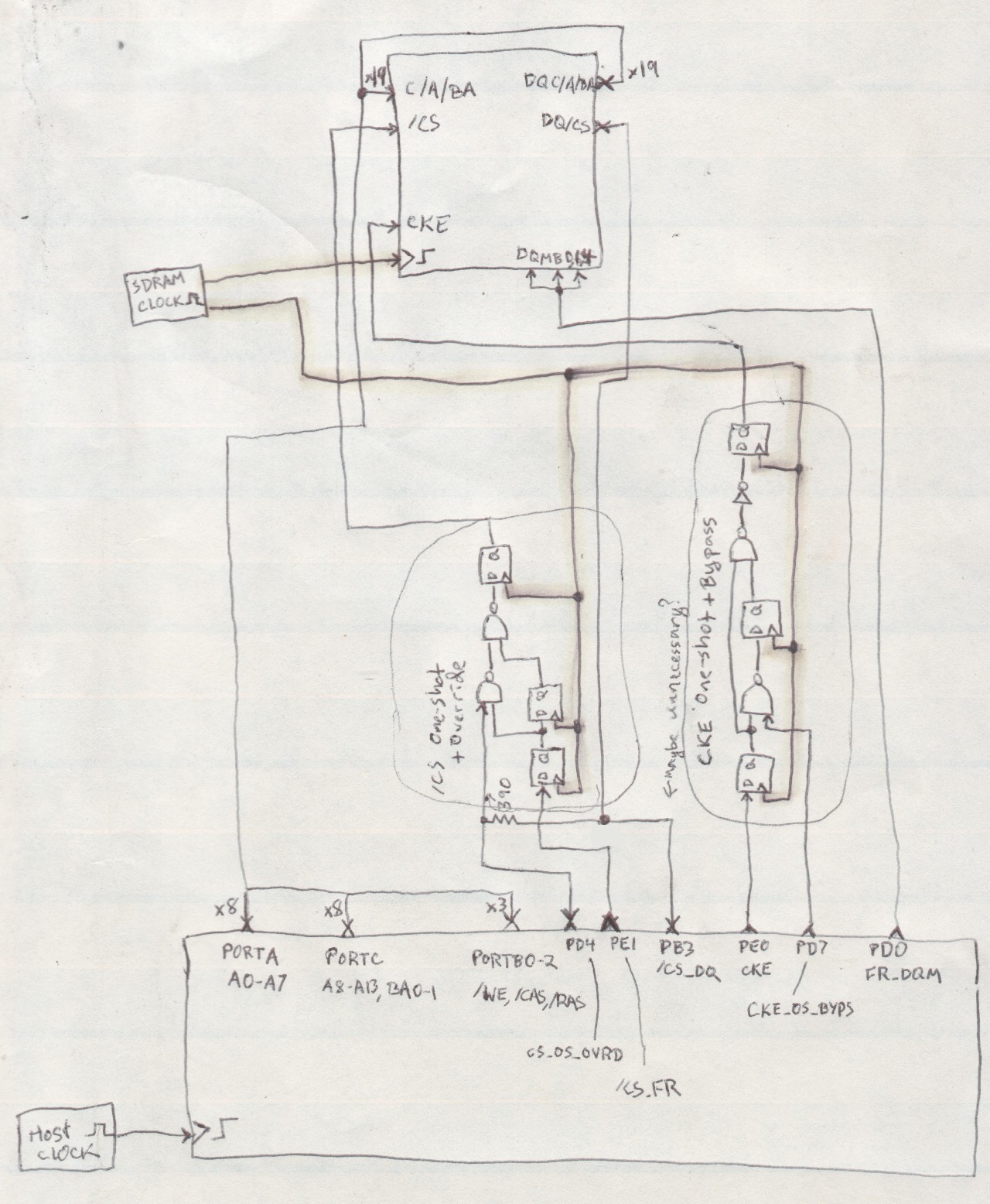
That circuitry *requires* some of those D-Latches to function, but there are some extras thrown in there for the purpose of more-predictable gate-delays. E.G. the CKE-One-Shot circuit could've just as well been designed such that the first NAND could've been on the Q side of the second latch, in which case the first latch could've been removed, entirely. But, then, there would be two gate-delays... The inverter after the second NAND could've, probably, been put on the output of the third D-Latch, but there are also long wires going between that circuitry and the SDRAM (just because of my wonky breadboard layout), so maybe it's better to have all the expectable delays *before* the last latch... (And maybe it'd be wise to throw another latch between that NAND and that inverter).
(Note, also, I didn't actually use an inverter chip, I used another 2-input NAND... Often when treating NANDs as inverters, schematics will show tying the two inputs of the NAND together, and tying that to your input-signal. I'm not *certain* about this, but I *think* it's better if you tie one input of the NAND to 1, then only toggle *one* input of the NAND with your signal... That might reduce the potential for glitching, etc.)
-----------So, now, I'm working on the Trigger circuitry. This has been described in a previous log...
The logic is long... several gate-delays involved. (And I've yet to convert it to my preferred NANDs, and I'm not sure whether using a diode and pull-resistor is really the best way to create a latch...)
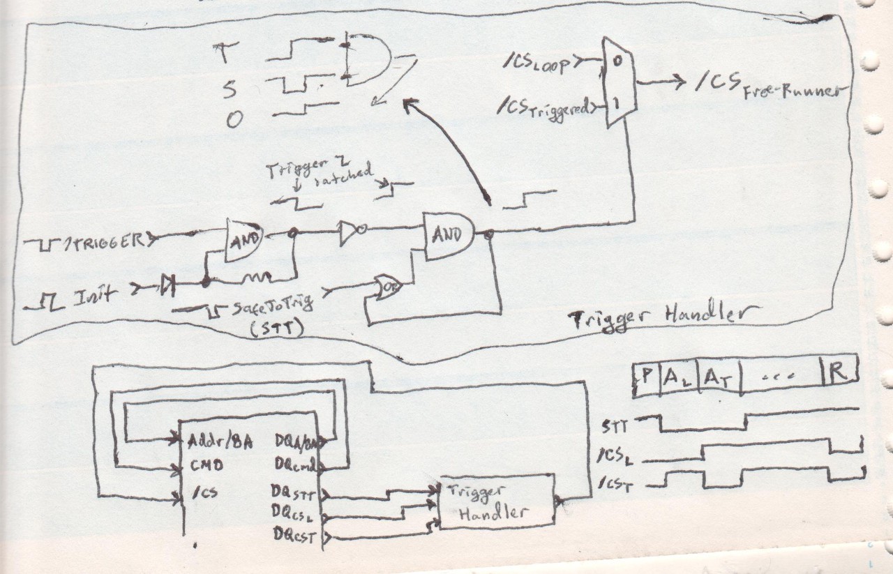
The purpose is to have a circular pre-buffer *before* the trigger. The SDRAM will "Free-Run" in a short loop until the trigger signal is received. When the trigger's received, a MUX will choose an entirely different set of "Free-Runner" commands, causing it to jump out of the loop. The problem is that there are some very rare instances where it's not safe to switch that MUX, so there's a "Safe-To-Trigger" input which adds another layer of logic, another layer of gate-delays...
And, as described earlier, those gate-delays may be somewhat unpredictable.
So, an option is to throw a D-Latch or two somewhere in there... There are three "layers" of gates, in that drawing, before the MUX, so 3 D-Latches could be in order. Another might (cautiously) be thrown between the second AND's output and the OR, or between the OR's output and the AND... One between each stage.
Depending on *where* the D-Latch(es) are inserted, we might have to shift that "safe-to-trigger" signal one or two clock-cycles prior. Just as adding a few latches between the One-Shot logic causes a (predictable) delay. Adding these D-Latches assures that as long as a single gate is faster than the maximum clock-rate, we don't have to worry about the somewhat-unpredictable propagation delays *at all,* thereafter...
Maybe "Pipelining"?
So, in the long-run, we should still be able to achieve 133MS/s, even if a single gate in the glue-logic is *barely* fast enough to keep up, even when we need multiple layers of glue-logic that's *barely* fast enough to keep up.
Anyways, throwing a latch after the gate, where that latch is clocked by the "system" clock... might be a handy technique... It's probably wasteful in a *product*, especially at the silicon-level... D-Latches are quite a few gates, but at the least, for a hobbyist trying to squeeze every ounce of speed out of a project, it might just be handy.
AND-OR-INVERT DOES NOT EQUAL NAND-NAND-->NAND!
WTF was I thinking?
So... Assuming my brain is functioning more-correctly in that realm today, than it was when I wrote this log... This should be right...
Which means... AND-OR-INVERT is the *inversion* of NAND-NAND-->NAND or, more-like NAND-NAND-->AND or maybe NAND-NAND-->NAND-INVERT Wee!
Which explains why my timing-diagrams weren't working out tonight... I'll be throwing a log up of that, later.
The rest of this log... should be right-ish... I think, yahknow... sorta, maybe.
Some updates, soon, on the trigger-circuitry, which if I can rewrap my head around this NAND-NAND-->NAND thing, might be greatly simplified... That'll be in the next-ish log.
Discussions
Become a Hackaday.io Member
Create an account to leave a comment. Already have an account? Log In.