 rolmie
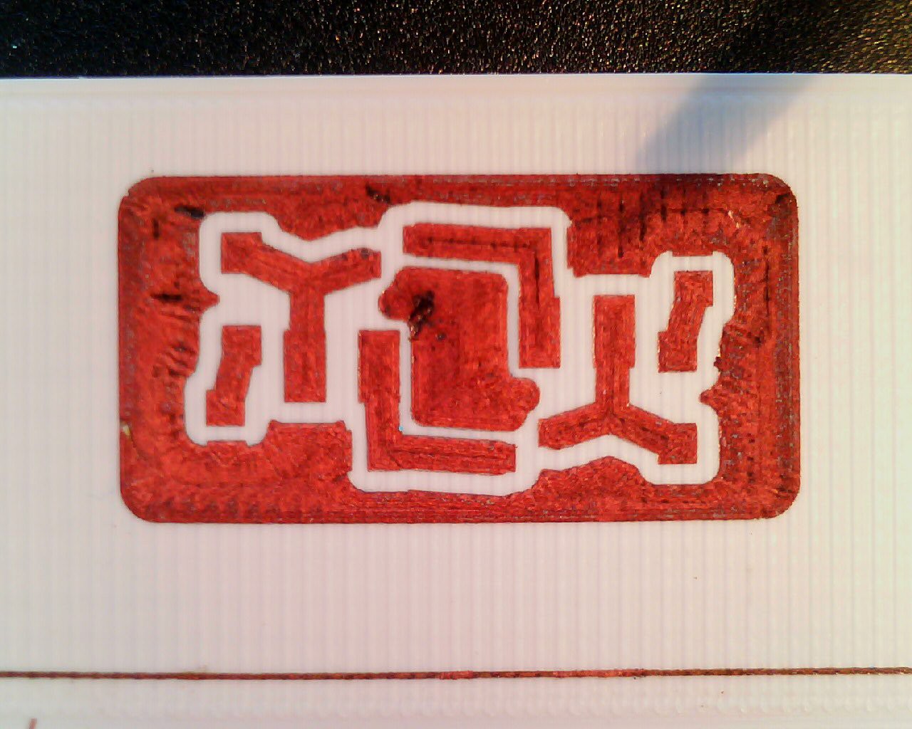
The dimensions are about 2.5cm x 1.25cm (1"x0.5"). The features and footprints are well 'hidden' in somewhat oversized traces, but this is an easy way to reduce resistance.
Printing strategy is to print as many "shells" as possible, as I suspect that conductivity along the printed lines is better than across. Additionally each layer is cured twice, interleaving the lines. The laser spot is about 0.1mm in diameter, the feedrate is 33mm/s. Curing a single layer at this size takes about 4:30 minutes.
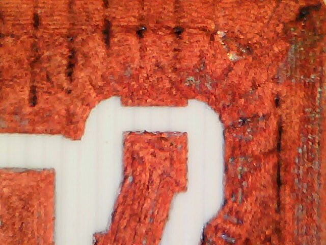
A well hidden SOT-23 footprint.
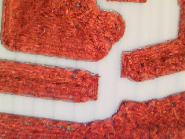
A 0805 foot print for a resistor:
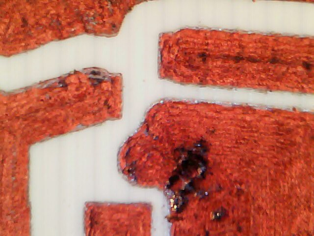
A "defect", reason unknown
Discussions
Become a Hackaday.io Member
Create an account to leave a comment. Already have an account? Log In.