-
Main board layout
05/13/2017 at 15:30 • 0 commentsStill working on the schematics. A lot of little details must be handled:
- splitting clock signals, in order not to overstress relay contacts
- program counter is 12 bits, add 4 bits and a selector knob to switch between several programs in two 64K x 8 flash chips
- how to get the program in flash... provide connector for dedicated AVR-based programmer with RS232/USB connection to PC
- The dedicated programmer should have buttons for manually composing an instruction and execute it
- The clock signals must be made. Clock must be started and stopped.
- User input buttons must be handled
- The remaining pcb's (except main pcb) will be made smaller than the first ones, now I discovered that 10 x 10 cm boards are a lot cheaper than bigger ones (at certain pcb makers).
- How to distribute the remaining circuits over several pcb's, and how to allocate signals on the 96 pin connectors
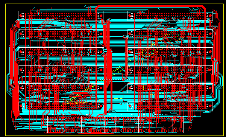
The last point has great influence on the routing of the main board. So, the main board is routed first. The connector allocation can still be changed if needed (except for the existing register and ALU pcbs). Here is the current status:
![]()
There are two rows of 6 connectors. At the front, there are 12 displays. The yellow signals must still be routed. But there will be more to do, since the schematics are not complete yet. This will keep me busy for a while...
The ALU has now all 8 bits built, and is working after solving a few soldering issues.
-
PCB's for ALU and registers
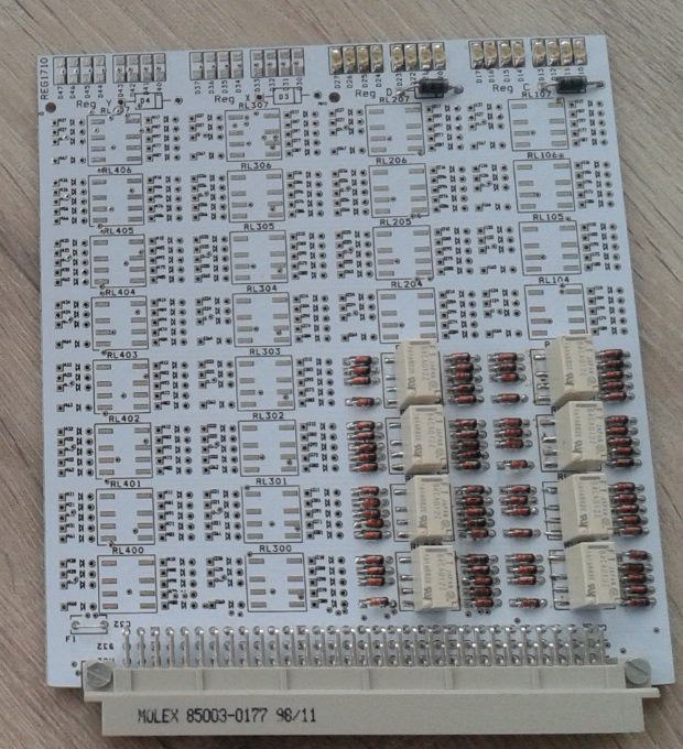
04/16/2017 at 19:13 • 2 commentsThe first two PCB's have arrived ! This is the pcb for the registers:
![]()
The pcb implements four 8-bit registers (registers C, D, X, Y). Only 8 bits (4 bits in 2 registers) are mounted. At the topside of the PCB, you see that each register has its own 8 LED's to indicate the contents. The pcb is labeled "REG1710" (top left) meaning the design is from 2017 week 10.
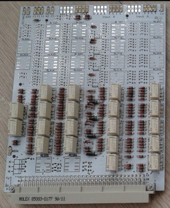
The other PCB is the 8-bit ALU "ALU1710":
![]()
Only 4 bits of the 8-bit ALU are mounted. The 4x4 relay section is the basic ALU, that includes two input registers (latches, to be honest). The sections with 2 relays are for the ADD-6 section and decimal correction. On the top of the pcb you see LEDs for input data, output data, function selection and flags. The ALU has the normal Load, AND, OR, XOR, binary ADD, but can also ADD decimally and convert BCD data to 7-segment display code. Subtraction needs help from outside of the ALU. It is done by inverting one of the register outputs (and setting the CY-input).
The placement system is all diodes and relays on top, and the resistors on the bottom. Relays are surface mount types, this gives more space for routing at the bottom. Diodes are through-hole 1N4148. I did not use BAV99 or other SOT23 types (otherwise I could be accused of using transistors secretly ;). Mini-Melf were also avoided since they tend to roll away when you try to solder them. Some signal wires drive many circuits, in that case the diode is 1N4004 or similar.
![]()
Of course, something was wrong. The connector DIN41612 was not close enough to the edge of the pcb (placement was based on the silkscreen of the footprint, I interpreted one of the silkscreen lines as the edge of the pcb, but that was wrong). I had to remove about 1mm of the pcb to make it fit. This destroyed only a few traces, that must be replaced by a wire.
Schematics and gerbers of REG1710 and ALU1710 are in the Hackaday files section.
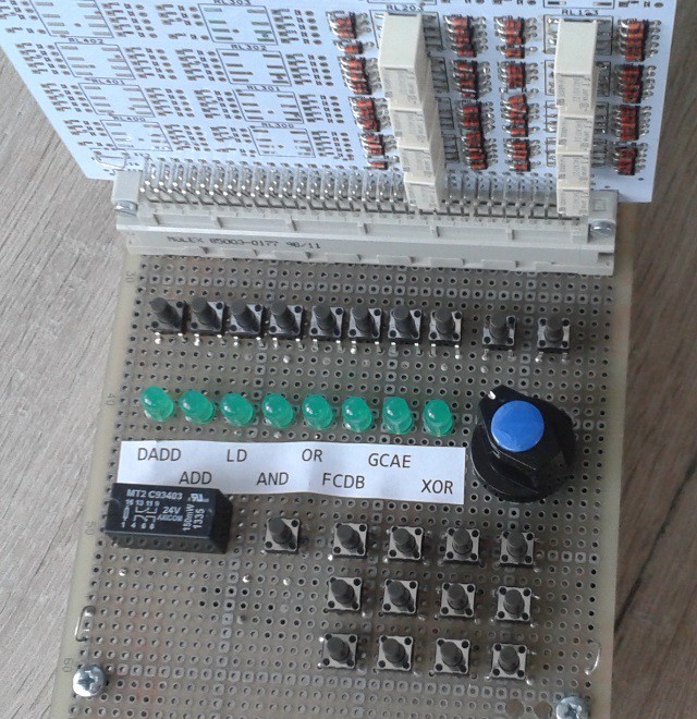
I did built a simple test device. The ALU and REG pcb's can be connected to it. The 3x4 buttons transfer data from a register to the input A of the ALU and from the ALU to a register. The 8 buttons on top control data on input B (next to it are a CLR input B button and a CY-input button). The big knob selects one of the ALU functions, the function is displayed by one of the green LEDs.
![]()
For the curious readers, here is the bottom side of the test device:
![]()
And of couse, I tested my new pcb's. Found a small problem:
It was intended that all diodes point in the same direction. But a few diodes on the ALU picked an older diode footprint, that had the silkscreen in the other direction. The result was a few diodes had to be reversed.
After that was done, all assembled functions were working ! (But the tester does not test the second output ports of the registers).
-------------------------------------------------------------------------------------------------------------------------------
Some new instructions were added to the instruction set:
- An instruction to load data from the program memory. The simulator has a unified memory, so the instruction was not needed there.
- Added XOR with immediate value
- Added a powerful instruction: Test a bit and branch. Within a single instruction, a single bit from a register pair can be tested, and a branch forward is done if the bit is 1 (or 0). In each register pair, the bits that can be tested are 0, 1, 2, 3, 4, 7, 15, 31. So this also replaces the clumsy sequence that was needed to test the upper bit of a value in a register. Instead of adding to the PC, this instruction can also conditionally add to register C. The branch forward has a reach of 31. In the instruction space, some space in the register-mode was sacrificed to make the test-and-branch possible.
Work will continue with the details of the control functions, and planning the "backplane".
-
New project: NeuronZoo
01/05/2017 at 15:31 • 0 commentsThere was not much progress for the relay computer lately, mostly because I was working on a new project called NeuronZoo ! The NeuronZoo project is on Hackaday now !
-
Schematics of 3 pcb's
12/18/2016 at 20:42 • 0 commentsThere was not much progress the last months, mostly because of a new project that I hope to show soon.
I have new ideas now about the distribution over several pcb's. Each pcb will have a DIN41612 96-pin connector to a backplane. For several subsystems, it is very easy to get over 96 signals, so reshuffling was needed. Also there is a limit to the number of relays that will fit on a pcb, the maximum is now 40. The size of the pcb's will be approx 10 x 14 cm.
- The register pcb implements 4 registers of 8 bits (32 relays). Of this pcb, 4 will be needed to implement the 7 16-bit registers (not all parts will be placed).
- The PC and decoder pcb. Implements 6 bits of the program counter (3 relays per bit), and circuits for decoding the registers. Two of these are needed for a 12 bit program counter, the decoder parts are not needed on the second pcb.
- The ALU pcb implements the 8 bit ALU, with both input registers A and B included. Two pcb's are needed for the 16 bit ALU.
- Instruction decoder
- Memory card. Two are needed, one for the program memory and one for the data memory. Includes the data shifter.
- The backplane will have connectors for all mentioned PCB's, and will hold the displays and buttons for the calculator. There will not be a straight 1-to-1 wiring of all connectors, every card will only work in its own position on the backplane.
For pcb's 1,2 and 3 I did put complete schematics in the Hackaday file section. The PCB design is almost complete for registers and pc/decoder, and halfway for the ALU.
The instruction set was again changed. Only half of the registers had logic instructions, this turned out to be impractical. Now, all registers have the same instructions. The price to be paid for this was that conditional instructions are now only for the PC and not for other registers (The ARM-like conditional instruction were not needed so much). In the Hackaday file section, the architecture and instruction list were updated. (My doc-to-pdf converter has trouble with the lines around tables, sorry about that).
-
Instruction decoder
05/24/2016 at 20:41 • 0 commentsIn this log I give some schematic info. I will explain the principles of the instruction decoder. (The ALU and registers are already discussed in one of the files).
In the HAD files section, the schematic RRC1613.pdf is a “summary” of the total design. There may be differences between the descriptions. It is hard to keep everything in sync as long as the design is not yet final.
Above the long line of RRC1613.pdf, you see the data path essentials for 1 bit (register and ALU). Below the line, the essentials of the instruction decoder are shown. The schematic is intented to give an overview of the polarities and pull-up/pull-down capabilities of the signals.
The clocking is not yet in the drawing. For every instruction there are four phases:
- 1) Called PH1 in schematic. Write to relays of register latch 1 group (CPU registers)
- 2) Write to relays of "Next state function 1"
- 3) Called PH3 in schematic. Write to relays of register 2 latch group (like the ALU input registers)
- 4) Write to relays of "Next state function 2", like the carry relays and logic result relays.
Phase 2 and 4 are not clocked, they are are direct result of the actions of phase 1 and 3.
At the lower left, you see the relays of the instruction register:Y0 Y1 mode zpage/immediate/memory/register
A1 A0 addressregister / src register
R2 R1 R0 dst register
M2 M1 M0 operation codeThe upper contacts of these relays are for the hold function, and deliver the signal (sometimes also in inverted version) for further decoding.
Actions for decoding phase 2 and 3 of the instruction:
The lower contacts of these relays are for decoding that has to take place immediately (to decide what data to put in ALU A and B registers)
Relays R2, R1, R0 select 1 of the 8 registers at output port 1 (via resistors at left and right above the ADD-6 circuit).Relays A1 A0 select 1 of 3 registers at output port 2 (via lowest contacts in the register bank, with pull-up signals "to_addr"). ( The architecture doc specifies 4 address registers, but the implementation has only 3.)
Relays "A0 slave" and "subtract" select 1 of 2 register pairs (register X or Y) for register mode on port 2 (it uses pull-down signals). The register pair is 32 bits, the shifter selects 16 bits out of these 32 bits (in 4 bit increments). The subtract relay chooses between normal or inverted output at port 2.
"A0 slave" means that this register has the same function/state as relay A0, and it is controlled by a contact of A0 so it switches a little later than A0 itself. This is no problem here because the shifter does not introduce a delay, so the register data will be in time to be loaded into the ALU_B register.
But when A1 and A0 select an address we can not use a slave register, because there is an extra relay level for address decoding (for capacitor-RAM or diode-ROM, not needed in the case of solid state memory). After the address has been decoded, the data will be immediately available to be loaded in the ALU_B register.
A capacitor RAM will be similar to Rory Mangles TIM8 design. Refresh will be different, the idea is that after the cap has activated the relay, it will immediately be refreshed through the hold function of the relay. The circuit of the caps will be such that there is no need to switch between discharge and charge.
Generation of control signals for the shifter and immediate addressing is not yet on the drawing, but this is not very difficult because the timing allows to use an extra level of relays here. Also the Store function is not on the drawing.
Relay Y0 selects if the A0/A1 selection is a pull-up (to 24V, address selection for memory mode) or a pull-down (to 0V, for register mode). Relay Y1 simply disconnects the address selection for Z-page mode, so for Z-page mode only the displacement is connected to the address (bits A0/A1 are not used, in contrary to architecture doc).Actions for decoding phase 4 and 1 of the instruction:
Decoding for phase 2 is less difficult, because there is time for 2 extra relay levels. At the left side you see the ALU-function signals F3, F2, F1, CY-enable, decimal, Carry-in. When all these relays are inactive, the LOAD function is selected as default. For a ADD function, the relays are set for logic XOR (F1 and F2 active) and CY-enable. For decimal ADD, the same is selected, and in this case also "decimal" is activated, to enable decimal correction in the ALU. ( For decimal ADD, in phase 1 the ADD-6 function is activated).
For logic functions, F1, F2 and F3 are set to correct position.
At the middle low side, there is a decoder that generates control signals to store the ALU result in one of the 8 registers. This is the same register as the register that was output on port 1 of the register bank. Conditional instructions simply disable this signal when the condition is not true.Incrementing the PC is not yet in the schematic. The incremented PC is always written back to the PC, except when the ALU delivers the new PC contents (in case of a branch or jump).
-
3rd log, about log
05/22/2016 at 21:07 • 0 commentsI've been busy with the log(x) function. It works quite nice, see CALC_6.TXT. The simulator counts the cycles between key presses, the log function takes 271 cycles for log(2) .
The ln(x) is calculated with the log function, as log(x) * ln(10). This is slower because the general multiply function is used after the log(x). The ln(2) takes 413 cycles. (So to reach my 10-second calculation goal, at least more than 40 instructions per second must be executed).
A faster, native ln(x) was also built but abandoned, to save program space.
The 10^x function is also in CALC_6, but is not yet accurate enough and only handles a small range at this time.
After the sin/cos/tan functions are also available, I will put the program in the logisim simulator to test everything on the gate level (eh.... coil and contact level).
And about the hardware.... it is expected to have approx. 270 DPDT relays.
-
First programming
05/16/2016 at 14:31 • 0 commentsStarted programming in the new assembler.... it didn't go very fast. One of the reasons was, that there were still some bugs in the assembler and simulator. Also I made some changes in the instruction set because some features were missing, like a bit test instruction (TSTB). The CL, DL and DH registers were given more functions, at the cost of functions for the X and Y registers.
Floating point number entry was more difficult than floating point multiply....
All files are now updated to the newest version. You can paste the CALC_4.TXT into the simulator to see the floating point number entry, add, sub and multiply.
Next thing that I will do, is make LOG and 10^x functions. (I will use the method of An Wang, inventor of the LOCI calculator).
-
Javascript online assembler and simulator
04/24/2016 at 19:39 • 0 commentsI have made an assembler and simulator in Javascript, (I modified the assembler-simulator from Marco Schweighauser).
The simulator includes a calculator display and keys. You can download it from the file list, or try it online at: www.enscope.nl/rrca
The first program is a 8-digit calculator that can only add. You can paste the following code in the online assembler, assemble it and start the simulator.
; CPU simulator test.
; Only calculates:  A + B =

 NOP ;first instruction is skipped !
clr:
plus:
  LDL Y,X	; save X in Y (32 bit)
  SUBL X,X	; clr X  (32 bit)

waitkey:
  HLT ; wait for button press
;  HLT ; option for switching to single step

  TEQ CL,'+'
  BRZ plus
  TEQ CL,'='
  BRZ result
  TEQ CL,' '  ;  CLR pressed ?
  BRZ clr
  ADD CL,0xffd0 ; keep digit code (subtr 0x30)
  ADDL X,X ; shift X one digit left
  ADDL X,X
  ADDL X,X
  ADDL X,X
  ADD XL,CL ; add new digit at the right side
  BR waitkey
  NOP        ; delay slot: the instruction after BR is also executed !

result:
  DADDL X,Y  ; 32-bit decimal add (Decimal ADD Long)
  BR waitkey
The architecture document was changed on a few minor points: The name of a few instructions changed, and the position of some bits in the opcode changed. There are a few new instructions in the above code that are not yet in the documentation: HLT and NOP.After a calculation, press the "clr" button before a new calculation is started.
Change the code and build your own calculator online ! You can also use scientific notation: two digits of CL are displayed as exponent, and the upper bits in CL control minus-signs and a decimal point after the first digit.
The page does not save your modified code, so you have to do some copying.