 Alex
Alex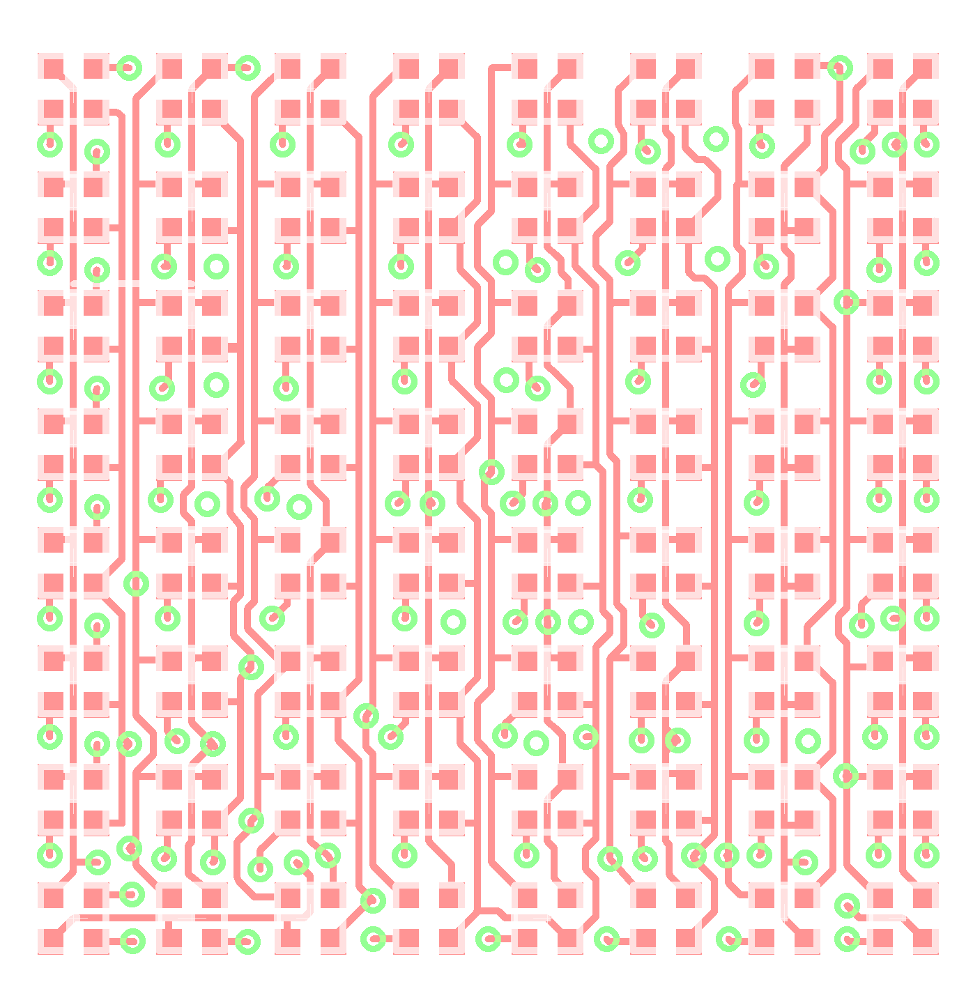
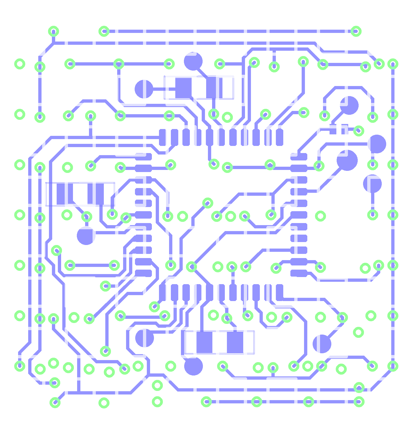
The two inner layers are not shown, but there are mostly just two planes for Vcc and GND and not many traces.
I am planning to use OSH Park's 4 Layer service for a first prototype. But first there are some thinks to do:
- find a oscillator, crystal or resonator that is small enough
(I think the size 2016 will fit, but not tested yet) - Clean up both silkscreen Layers
Discussions
Become a Hackaday.io Member
Create an account to leave a comment. Already have an account? Log In.