 Szoftveres
Architecture
Wikipedia article:
Transport Triggered Architecture
Since the CPU doesn't utilize microcode (I don't have an EPROM burner so one of the goals was to create the CPU without EPROM chips), it can do only one simple thing: move data during each instruction cycle from the data source to the destination. Eventually each CPU instruction is a hardwired MOVE instruction, the instruction code itself determines the component that will be the data source (e.g. accumulator, input port, RAM, program memory, etc...) and the data destination (accumulator, adder, inverter, output port, program counter, etc...).
During the execution phase, a data source component is signaled to place its data on the internal CPU data bus, and a data destination component is triggered at the same time to latch this data. A simple example is the 'JUMP' functionality; the CPU instruction logic triggers a data source component to place its data on the internal data bus, and triggers the program counter at the same time to store this data.
The only drawback of microcode-less design is the lack of more complex CPU functions (stack, interrput handling, etc), however stack can be emulated with software: I use one of the uppermost bytes in the RAM as a stack pointer, and have implemented assembly macros for PUSH, POP, CALL and RET. I'm currently able to write complex C programs with arbitrary deep function calls for this CPU using my C-like compiler.
Internal structure
CPU control logic
The CPU control logic consists of 4 components:
- CPU phase logic
- Program counter (PC)
- Instruction register
- Instruction decoder
CPU phase logic
The phase logic is responsible for providing phase signals to the CPU. One CPU instruction cycle is constituted of 4 CPU phases regardless of the instruction length (1 or 2 bytes). Two of the 4 cycles are IDLE cycles, primarily responsible for preventing glitches during the transition from 'fetch' to 'execute' phase. The phase circuit is constructed by using a 2 bit counter (74HC74).
CPU phases:
0. Idle
1. Fetch
- signal the program memory to place the next instruction word on the CPU internal data bus
- signal the instruction register to latch and store the instruction word
- increment PC
2. Idle
3. Execute
- activate instruction decoders to execute the instruction by activating /OE and /WR signals on the selected data source/destination components
- increment PC if the data source was the program memory
Waveforms of phase signals during each phase (refer to the schematics, I intentionally swapped inverted- and non-inverted prefixes):
Phase LSB
--------+        +--------+
        |        |        |
        +--------+        +--------+
Phase MSB
-----------------+
                 |
                 +-----------------+
Inverted MSB
                 +-----------------+
                 |
-----------------+
    0.      1.       2.       3.
Program counter
The program counter is composed of parallel-loadable counter ICs (74HC161). Actually the schematics contain only 2 of them, but I extended the real implementation to use 4 of them, so the program memory space is eventually 64k. In order to load data into the higher 8 bits of the PC, an extra latch IC (74HC574) was added. This latch has to be loaded with the MSB prior to each JMP instruction, the content of it is loaded into the higher (MSB) counters at the same time when the lower 8 bits are loaded directly from the CPU internal data bus.
The PC is incremented automatically after each read from the program memory (fetch cycle, or reading literal data from program memory).
Instruction register
The instruction register is an edge triggered D latch (74HC574), this register is loaded with data during each 'fetch' cycle. The easiest way to imagine the fetch cycle is as a special hardwired MOVE instruction; the data source is always the program memory and the data destination is always the instruction register.
Instruction decoder
The instruction decoder is composed of two demultiplexer ICs (2 x 74HC138) and is driven by the instruction register. A CPU instruction...
Read more »


 ammarbhayat28
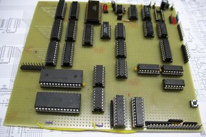
 jaromir.sukuba
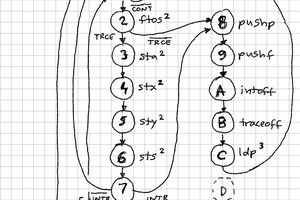
 zpekic
 Reed Foster
Regarding your software solution to the missing stack: the old Intel 8008 CPU was also missing a stack. Hal Chamberlin wrote an article on how to add an external stack to the 8008. This was in the second issue of Byte Magazine (https://archive.org/details/byte-magazine-1975-10/page/n53/mode/2up, page 52 - or page 54 of the PDF.) He used a couple of 7489 16X4 SRAM chips, and only took seven chips, plus a couple of optional inverters to ensure that the selects are at active low levels. You can replace the 7489s with a single 6116 2KX8 SRAM chip, and add two more 74193 (datasheet: https://www.ti.com/lit/ds/symlink/sn74ls193.pdf?ts=1623867018114&ref_url=https%253A%252F%252Fen.wikipedia.org%252F) counters chained to the original '193. This will give you a 2K byte external, hardware stack for a pretty low cost (both price and PCB real estate.)