 Ted Yapo
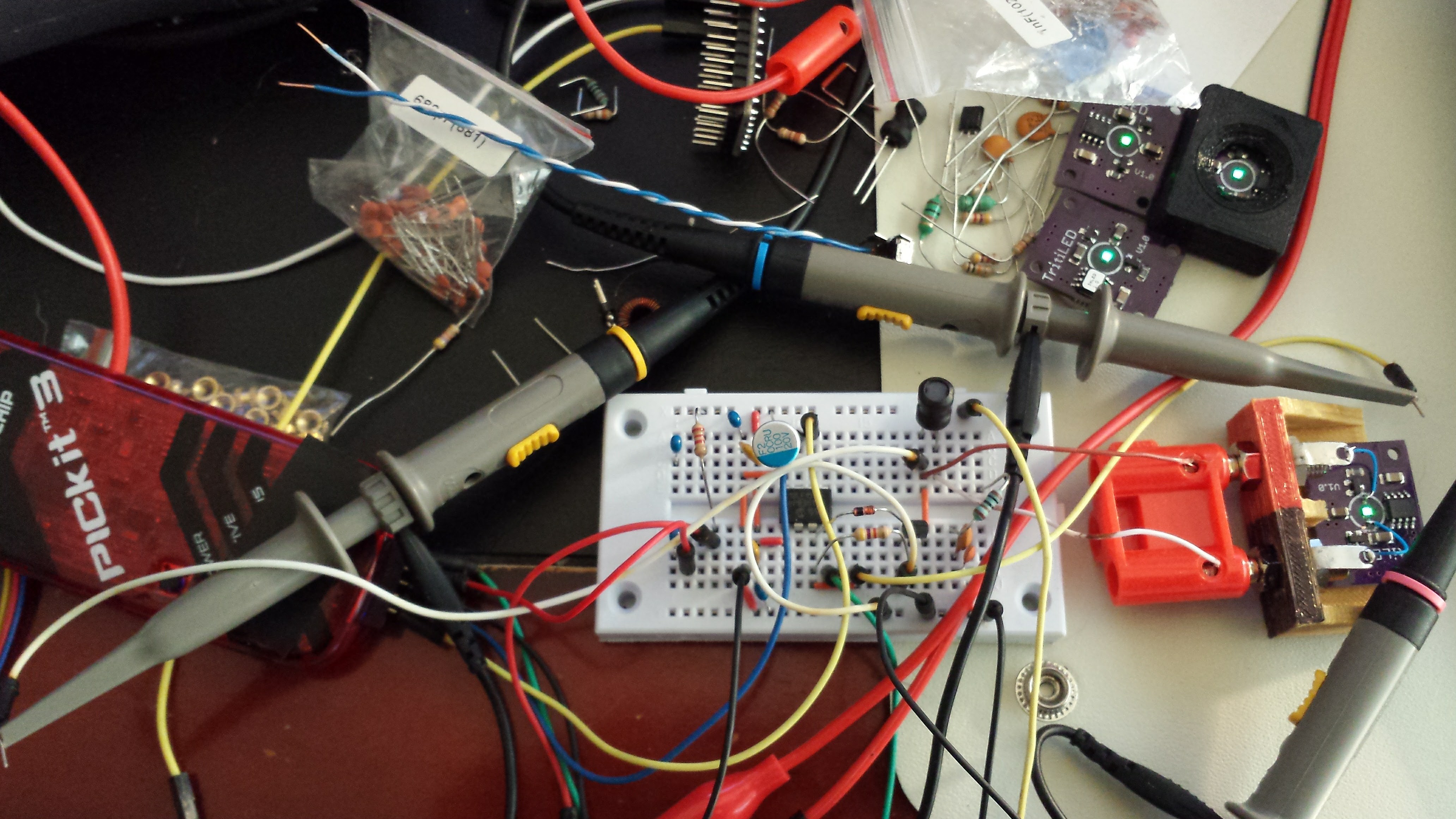
I breadboarded a first cut at a more efficient circuit this past weekend. Consensus is that it appears a little brighter than the 1.0 circuit (not measured with the camera yet), and a back-of-the-envelope estimate says it will run for two years on a CR2032 battery (a better analysis is coming in the next log). It consumes 49% less current than V1.0, and can be made to blink bright flashes instead of a constant glow while maintaining the same current draw. The circuit incorporates some good ideas suggested by Jaromir and Tony. Here's the mess of a prototype:
Pulse Circuit
The design started with an analysis of the efficiency of sawtooth current drive waveforms for the Luxeon LED, as I did for a 5MM LED earlier:
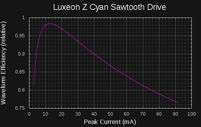
With sawtooth waveforms like those produced by the inductor-LED circuit I had simulated before, the best LED efficiency is seen at around 13 mA peak current. After a little experimentation with PIC clock speeds and inductor sizes, I came up with this circuit that generates peaks of around 15 mA (roughly estimated from peak LED forward voltage and the measured I/V curve):
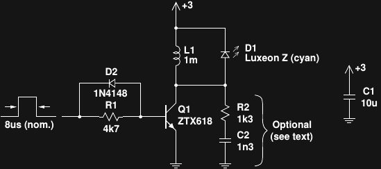
The design is based on discussions I've had with Tony about single-shot boost converters, and it works pretty well, as long as the LED doesn't have a reverse-protection diode inside (this one does not). A 1 mH inductor is huge for a switching power supply, but all of the four different through-hole styles I had in this value worked in the circuit to some degree. One was superior, though - I will need to find an SMD version with similar properties. As discussed earlier, pulses from the PIC turn on the transistor to magnetize the inductor, then the inductor "discharges" through the LED to create the light pulse. For these tests, I used a modern PIC as suggested by Jaromir. So far I've only used a PIC12LF1571 I had on-hand; I am also going to try a PIC12LF1552 which is supposed to have a slightly lower sleep current.
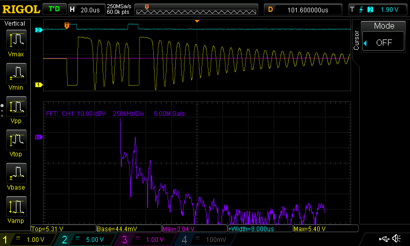
The ZTX618 is an awesome transistor (at a premium price), with super-high beta and super-low Vce(sat) - evidence of this can be seen in the waveforms below, where the collector of Q1 drops to 38 mV during the pulse. The high beta allows a high value for R1, limiting the wasted base current. D2 is critical to achieving high efficiency with this circuit - without it, Q1 turns off slowly, wasting power at the critical peak inductor current. Here are the waveforms observed at the input, driven by a single PIC output pin (channel 2, cyan), and at Q1's collector (channel 1, yellow). The supply voltage of 3.04 V (channel 3, magenta) is shown at the same offset as channel 1.
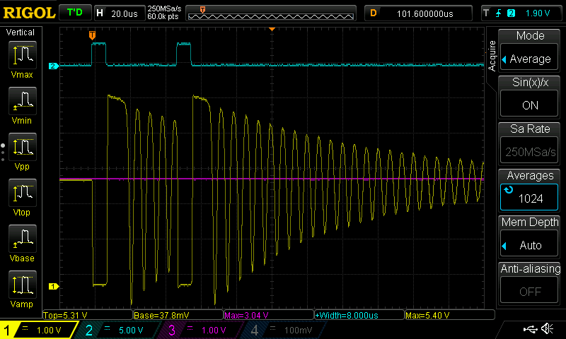
Two things are immediately apparent. First, you can see the trick to lighting LEDs with these small current pulses - use multiple pulses every time the PIC wakes from sleep. Here, the PIC is waking every 16 ms to output two pulses. Waking every 8 ms to output a single pulse is less efficient because of the overhead involved in starting the PIC clock each time. Waking less often to generate more pulses is even more efficient, but the blinking becomes noticeable. Push this far enough, though, and you get a very brightly flashing beacon at the same power. Pulsing the LED 128 times every 1 second produces a nice attention-grabbing display using around the same average current.
The second thing evident is that the circuit rings like a bell after each pulse. The delay between the pulses is actually chosen to coincide with the ringing, so that the next pulse starts on the down-swing of the oscillation. Fine tuning this delay seems to add a few percentage points of efficiency. You can see the spikes in the spectrum at 145 kHz and the second harmonic at 290 kHz here:
A PCB made for this circuit probably wouldn't make an efficient radiator for these LF frequencies, but since one of my hobbies is hunting LF navigation beacons, I wanted to clean this up. I had previously dealt with this kind of ringing in another circuit following the advice in the Ti Applicaton Report SLPA010 "Reducing Ringing Techniques for NexFET High-Performance MOSFETS," so I gave the same approach a shot here. Some cut-and-try analysis provided the values for R2 and C2, which form an RC snubber network across the output. With those parts in place, the ringing is greatly reduced:
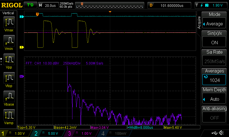
Unfortunately, this also reduces the efficiency of the circuit by 10%. When I design a board for this version, I'll include sites for these parts and decide afterward if they should be populated based on some (probably crude) emissions testing.
Performance
I haven't used the camera method to compare the brightness of this circuit with the V1.0, but I think it's brighter - two other people have agreed. One of the complications is that this version produces a longer-wavelength output because the LED is driven with lower current. This may also complicate the camera comparison method, but at least I'll have some objective data on the comparative brightness.
As for current draw, here's a summary of the two versions:
| Version | Current drain @ 3V | Estimated CR2032 lifetime (years) |
| V 1.0 | 26.3 uA | 0.95 |
| V 2.α (no snubber) | 13.5 uA | 1.86 |
| V 2.α (snubber) | 15.0 uA | 1.67 |
Here, the estimated lifetime was computed by dividing the nominal 220 mAh capacity rating of a CR2032 by the measured current draw at 3.0V. This under-estimates the actual run time because as the battery voltage drops, the circuit draws less current. I actually have a much better approach that models the battery capacity as the voltage drops over the lifetime of the cell to give more accurate predictions; I'll present it in the next log. Initial results of the new method show a run-time over two years for the new circuit.
Next Steps
As luck would have it, I found a DigiKey box on my doorstep this afternoon containing a few different types of 1 mH SMD inductors, low-Vgs MOSFETS, and PIC12LF1552's. I used a BJT in the first prototype because that's all I had for through-hole devices. The next step is to build an ugly-style prototype of the same concept to see how it works - for all I know the crazy parasitics in the solderless-breadboard version may be important circuit components :-)
I have a lot of PIC pins left over. This was convenient for the prototype, since I could just leave the programmer connected (except the Vdd line) during testing. It would be nice to have the pic programmable on the PCB, so I am considering adding card-edge contacts on one side of the board for the ICSP lines.
I'd also like to add a button to select maybe three different modes - continuous glow, fast flash, and slow flash, each of which maintains the 2-year battery life. Mostly, just I need to add some switch-debouncing code to make it work
Luminosity Standards
I would like to find a cheap, repeatable luminosity standard. Wikipedia provides some clues about a possible DIY version based on older standards:
One candlepower was the light produced by a pure spermaceti candle weighing one sixth of a pound and burning at a rate of 120 grains per hour.
My whaling schooner is in dry dock for repairs at the moment, so that one is probably out. Luckily, a newer standard was devised:
The candela is the luminous intensity, in the perpendicular direction, of a surface of 1 / 600 000 square metre of a black body at the temperature of freezing platinum under a pressure of 101 325 newtons per square metre.
Freezing platinum - I wonder if my refrigerator gets that cold if I turn it all the way down ;-)
When this project got blogged on hackaday.com, one of the commenters, [Paul] mentioned another possibility:
Though a great tool, unfortunately this device is useless for one of the best uses of a tritium light in astronomy: camera calibration. A tritium light source (e.g. from http://www.betalight.nl/ ), is an ultra-stable, zero-noise low-intensity narrowband light source ideal for testing and calibrating CCD camera sensors: https://www.google.com/search?q=betalight+ccd+testing
Now, if I could buy a betalight in the US (I'm looking at you, NRC), I would never have started this project!
There must be a way to do DIY luminosity calibration. Ideas, anyone?
PIC Source Code
For those interested, here's the source code I used for the tests. There are actually a number of different ways of generating 8us pulses - I found that one instruction cycle at a 500 kHz fosc was much more efficient than 8 cycles at a 4 clock MHz (CMOS!). You can change the watchdog timeout (e.g 1s), and the number of pulse pairs (e.g. 128) to produce bright strobes at the same average current draw. It's released here under an MIT license (I need to start a GitHub repository for this project!).
;;;
;;; single_shot_boost.asm : PIC12F1571 code for CR2032-powered LED glow marker
;;;
;;;  20160828 TCY
    LIST        P=12LF1571
#include    <p12lf1571.inc>
    ERRORLEVEL -302
    __CONFIG  _CONFIG1, _FOSC_INTOSC & _WDTE_ON & _PWRTE_OFF & _MCLRE_OFF & _CP_OFF & _BOREN_OFF & _CLKOUTEN_OFF
    __CONFIG _CONFIG2, _WRT_OFF & _PLLEN_OFF & _STVREN_OFF & _BORV_HI & _LPBOREN_OFF & _LVP_ON
        CBLOCK 0x70
            counter
        ENDC
        ORG     0
RESET_VEC:
        BANKSEL LATA
        clrf    LATA
        BANKSEL OSCCON
;        movlw   b'01101011'     ; 4 MHz osc
        movlw   b'00111011'     ; 500 kHz osc
        movwf   OSCCON
        BANKSEL TRISA
        movlw   b'101111'       ; RA4 as output
        movwf   TRISA
        BANKSEL WDTCON
;        movlw   b'000010101'   ; WDT 1s timeout
;        movlw   b'000010011'    ; WDT 512ms timeout
;        movlw   b'000010001'   ; WDT 256ms timeout
;        movlw   b'000001111'   ; WDT 128ms timeout
;        movlw   b'000001101'   ; WDT 64ms timeout
;        movlw   b'000001011'   ; WDT 32ms timeout
        movlw   b'00001001'     ; WDT 16ms timeout
;        movlw   b'000000111'   ; WDT 8ms timeout
;        movlw   b'000000101'    ; WDT 4ms timeout
;        movlw   b'000000011'   ; WDT 2ms timeout
;        movlw   b'000000001'   ; WDT 1ms timeout
        movwf WDTCON
N_PULSE_PAIRS  equ 1
MAIN_LOOP:
        BANKSEL OSCSTAT
        btfss   OSCSTAT, MFIOFR   ; check for osc ready
        goto    MAIN_LOOP         ; spin here until osc ready
        banksel LATA
        movlw   N_PULSE_PAIRS
        movwf   counter
PULSE_LOOP:
        bsf     LATA, 4        ; start inductor ramp-up
        bcf     LATA, 4        ; end inductor ramp-up
        nop
        nop
        nop
        nop
        bsf     LATA, 4        ; start inductor ramp-up
        bcf     LATA, 4        ; end inductor ramp-up
        nop
        decfsz  counter
        goto    PULSE_LOOP
        sleep
        goto    MAIN_LOOP
        END
Discussions
Become a Hackaday.io Member
Create an account to leave a comment. Already have an account? Log In.