 Samuel A. Falvo II
I plan on using this bus as the backplane for supporting R&D for my Kestrel Computer Project. Signals are as follows:
SYSCON Signals.
50MHZ. A 50MHz reference clock generated by the backplane. NOTE: This doesn't mean that the bus has to run at 50MHz; you're free to insert as many wait-states as needed to slow things down to a more manageable speed. In fact, considering the physical size of even the smallest backplanes, it'll be very difficult to pull off true 50MT/s performance levels. I think the best you'll be able to do is 25MT/s. Even so, all signals on the bus are synchronized to the rising edge of the 50MHZ signal.
RESET. This backplane-generated output is high while the whole system is still being configured. It will only go low once all cards report having completed their configuration.
CDONE. This signal is generated by the card, and is high if, and only if, all configurable components have completed their configuration cycles. For example, Lattice FPGAs (and I think Xilinx too) have a pin called CDONE which goes high when the FPGA has finished bootstrapping itself from configuration flash. Note that a card may, at any time, bring this signal low (e.g., as when a user pushes a reset button).
Common MASTER/SLAVE Signals.
D0-D15. A 16-bit, bidirectional datapath. Only the current bus master can drive the data bus; all other cards can only sense their current state.
A1-A31. A 32-bit bus providing an address to read or write from. Note that the state of A0 combined with the size of the transfer is encoded in the SEL(1:0) pins. Only the current bus master is allowed to drive these pins.
SEL1-SEL0. These two pins select which half of the data bus will contain valid data. SEL1 corresponds to D8-D15, while SEL0 corresponds to D0-D7. Only the current bus master is allowed to drive these pins.
WE. This pin distinguishes a read transaction from a write transaction (as viewed from the perspective of the current bus master). Only the current bus master is allowed to drive this pin.
ACK. When the bus master addresses a peripheral, the peripheral is responsible for acknowledging the transaction. Each clock transition between the assertion of STB and ACK is a wait-state. Only the addressed peripheral is allowed to drive this pin.
STB. When the current bus master commences a bus transaction, it asserts this pin. Otherwise, it keeps this pin negated. This pin can only be driven by the current bus master.
CYC#. When the current bus master wants to take control of the bus, it brings this pin low. The master basically owns the bus for as long as this pin is held low. This pin is not bussed; the master must drive this pin high if it's not the currently selected bus master. Slaves should tie this pin to +3.3V.
CYCA. (Cycle Announce.) If any slot's CYC# pin is low, regardless of slot, CYCA goes high. This tells the card that a bus cycle is in progress, and that all other master-driven signals are valid.
BCL#. Bus Clear. A bus master is allowed to hold onto the bus as long as it needs, or even wants to, as long as it respects this pin. Any other card that wants to be a master should assert this pin low. This pin is open-drain, allowing multiple cards to drive it. It must remain low as long as another bus master wants to conduct priority traffic. Otherwise, it's more polite to wait its turn.
BGO and BGI. Bus Grant output and input, respectively. When these two signals differ, the card is the currently selected bus master. When they're equal, then the card is not the currently selected master. If a card does not want to be the master this turn around, then it should reflect the state of BGI to BGO. Otherwise, it should assert CYC# and drive the bus as appropriate.
+5V and GND. These pins provide power to the card. Although +5V is the supply voltage, the logic signaling over the bus is 3.3V. Each card is expected to have its own voltage regulator.
DIN 41612 Pin Out.
        A       B       C
    1   D0      +5V     WE
    2   D1      GND     A1
    3   D2      +5V     A2
    4   D3      GND     A3
    5   D4      +5V     A4
    6   D5      GND     A5
 7 D6 +5V A6
...
Read more »


 techav
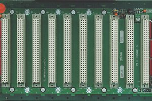
 Keith
Keith
 EtchedPixels
I'm sorry to rain on your parade but a bus is not simply a matter of joining the dots. If your bus is going to run at any decent speed, the bus wires will act like transmission lines. You have no specified bus impedance or terminators. You have no rules about what the bus drive or loads must conform to. How many bus masters and slaves can share a bus?