 Dan Kisling
The spectrum analyzer is an incredibly useful tool for any person dealing with signals. They allow us to see something a bit abstract, but quite useful: signals in the frequency domain. This has a variety of applications, such as radio, audio, and circuit analysis. Anything problem that can be solved by better understanding the spectra of the signal is the domain of the spectrum analyzer. My original fascination with these devices came from watching the spectra of the audio band for my favorite songs. I loved the visualization of the high notes and low notes in the spectra. This has inspired me to try to create devices like this in the past, though not full solutions. This project was chosen to finally create an all-in-one solution to a spectrum analyzer. The bonus is that we have found this project to be an exemplary review in all of our electronics learning. Everything from signal analysis to circuit design is heavily involved in this project. We ultimately want to create a product we would want to use. And we know we are not alone in this desire, so we are going to create a spectrum analyzer that is at a cost that is attainable by the hobbyist and the student.
Equipment for analyzing electrical signal spectra is inherently expensive. Equipment typically runs on the order of $50,000, with lower-end devices still costing on the order of thousands of dollars. Though expensive, these devices offer high resolution and operate in a wide range of frequencies. This is great for industry, where precision may be key, but the functionality is often over-kill for educational, hobbyist, or professional audio usage and the prices are likewise impractical. In addition, the user interface for many devices are hard to use, assuming the user has a working knowledge of spectrum analyzers, and requiring tuning and calibration. This combination makes spectrum analyzers inaccessible to hobbyist and audio electronics communities and a financial burden on educational institutions not requiring industry precision.
Inexpensive spectrum analyzers, costing under $500, do exist, albeit in smaller quantities than their more expensive counterparts, but do not remove the learning curve associated with the devices. The project proposed is a stand-alone low-cost spectrum analyzer, with a built in display, that supports a simple user interface. The physical device will be able to detect frequency spectra in addition to calculating total harmonic distortion and measure frequency domain noise. The interface will take advantage of presets, built calibration and tuning and intelligent parameter selection so user with limited knowledge of the device could easily utilize it. More advanced parameter settings will be exposed to the user as well for finer-tuned usage and to appeal to the more knowledgeable user.
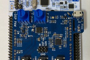
Below is a working prototype of our project.


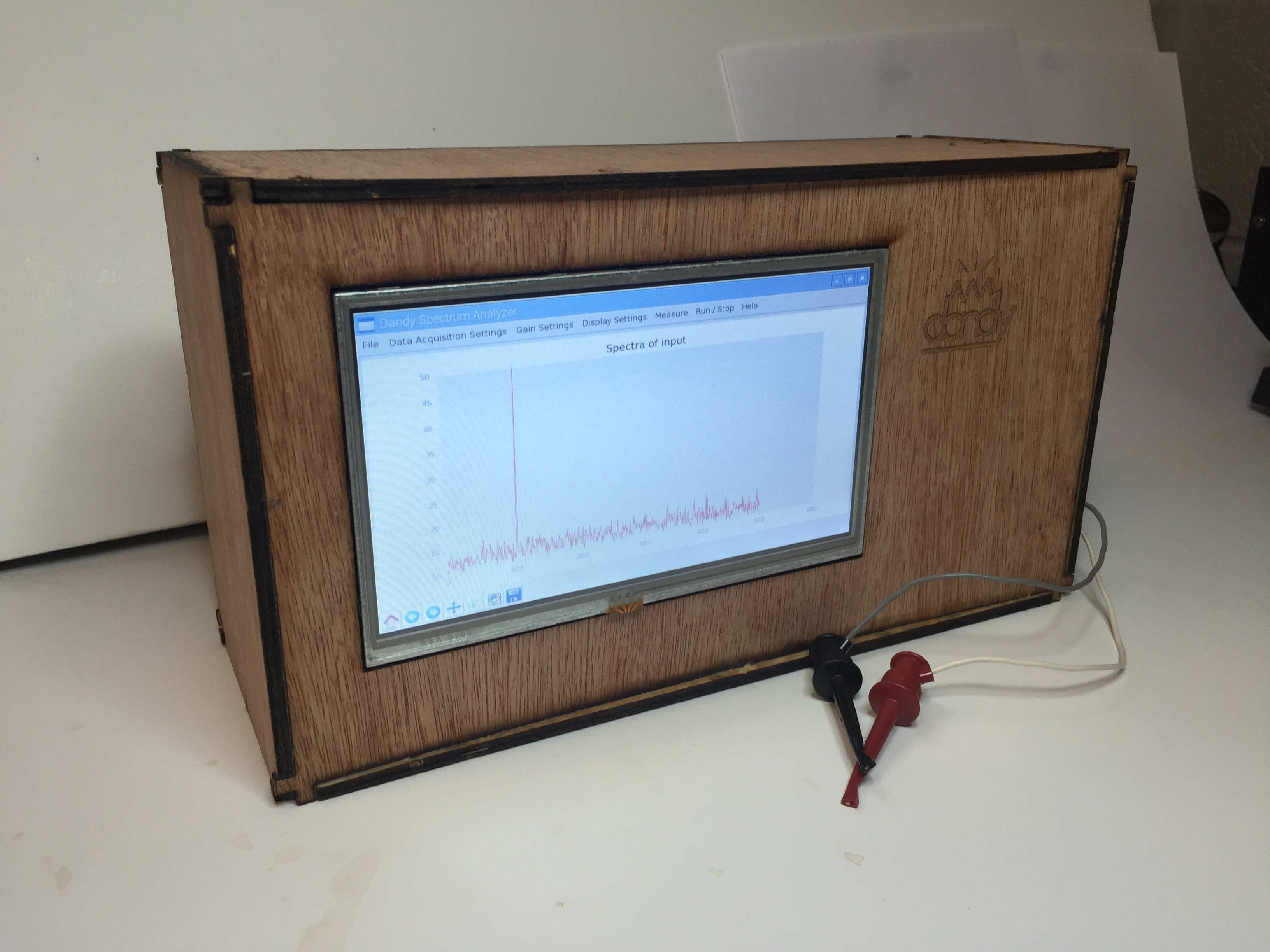
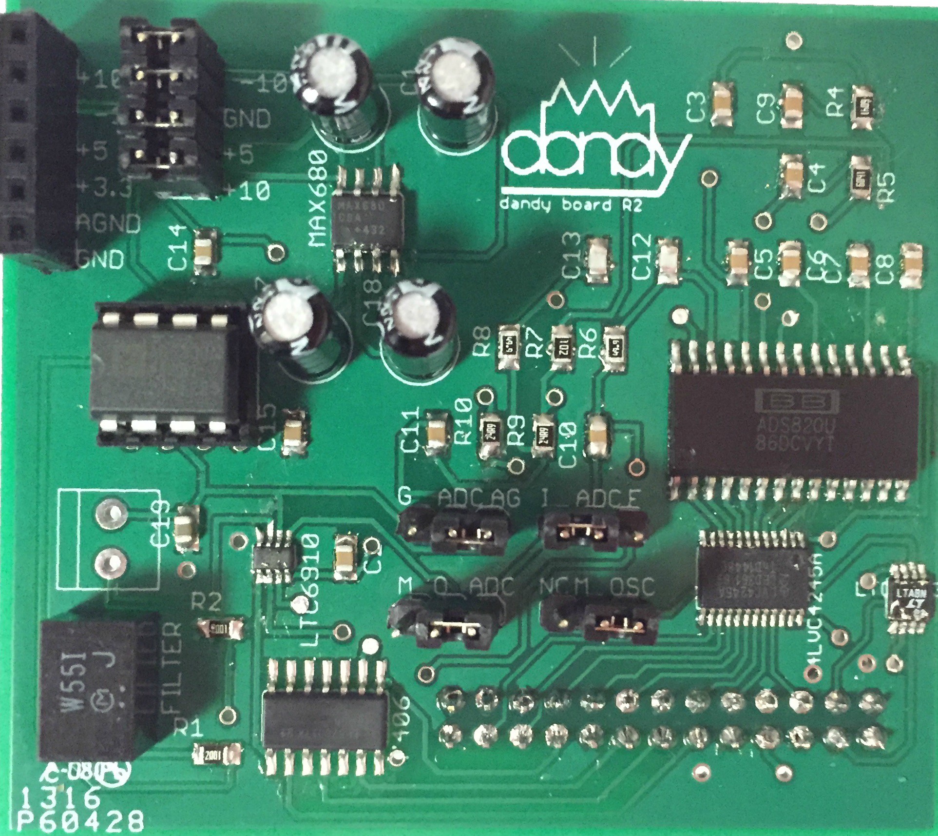


 After the bandpass filter, the signal is sampled by the ADC. Everything from there is done in software. The raspberry pi takes the samples and performs a GPU accelerated FFT on them, splices the spectrums together, and displays them in the GUI to the user. The user can then use the GUI to change some settings in order to capture the signal he or she wants.
 From left to right: My lab partner Andrew, Professor Frey, and me, Dan
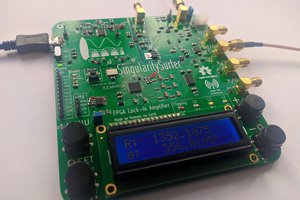
 SingularitySurfer
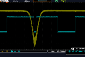
 Clyne
Clyne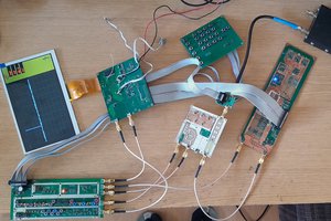
 michal777