agp.cooper
"PCB Isolation"? What is that?
Basically its macro that converts a printed circuit board (PCB) image into outlines that can be used by a CNC machine to make a copy of the board. As it only traces the outline of the PCB tracks (i.e. it does not remove all the copper) so its called an "Isolation".
Why not use an online 'Image to Vector' program?
Yes, they do a respectable job. Nicely smoothed but lots of points.
Really, writing the macro was just for fun!
Okay, how to use:
1 Convert your PCB image into a 24 bit uncompressed BMP.
2 Try an get it as Black and White as possible using an image processing
  software.
3 Put the macro in a directory (where you can find it).
  (the macro file manager will allow you to navigate anywhere to find
   your BMP)
4 Run the macro (mine is call BMP2DC.BAS).
5 The BMP File Viewer will appear:
   5.1 Select a BMP file (a preview will appear).
   5.2 Press Okay
6 Depending on the BMP file size, after a few seconds another menu will
  appear:
   6.1 Select your options (note: the pixel spacing is in mm per pixel and
       is used to scale the output to DeltaCad).
   6.2 Press Okay
7 Depending on the PCB complexity after a few minutes the macro will
  update the screen with the result.
The macro uses shapes (Blue for clockwise (or an outside edge) and Red for anti-clockwise (or an inside edge)).
If black outline may appears then number of segments is too high (>3072) for a shape.
A black box presents the image limits.
Note: All outlines are closed, to do this a one pixel border has been imposed/cleared (i.e. don't have anything on the border).
Cypress Enable is pretty slow, a lot of time was spent making the code efficient (all algorithms are linear or nLogn).
In C it would be lightening fast.
If you wondering it took three solids weeks to write this macro from scratch!
The only borrowed code was the BMP Preview file manager code that came from the Cyress Enable website:
http://www.cypressinc.com/demo.zip (BMPView.bas)
Workflow
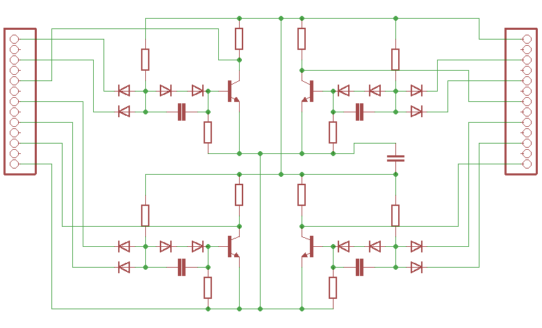
Draw your schematic (I used Eagle here):
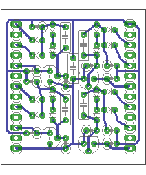
Convert to PCB (you will need this for component placement later):
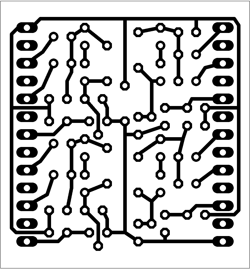
Export as black and white BMP (600 dpi):
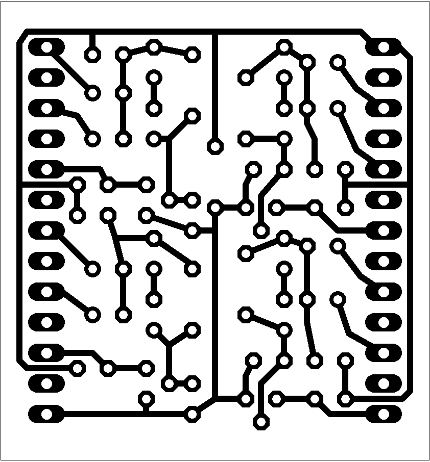
Mirror the image (as this is a top view) and convert to 24 bit BMP:
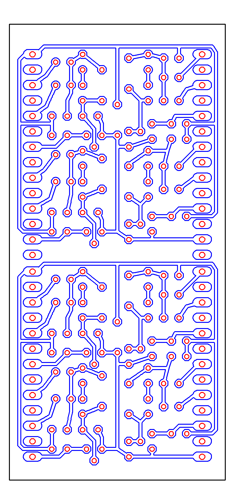
Run the macro (BMP2DC2) to import the BMP into DeltaCad.
In this case I duplicated the design.
Export as DXF:
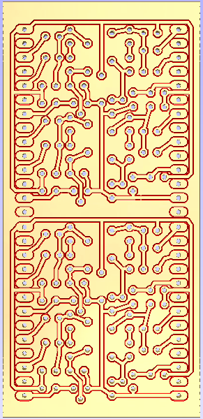
Import into a CAM package (I use Cut2D).
I used a 60 degree V bit (0.2 mm cut depth for isolations) and a 0.72 mm end mill for the holes and the cutout.
The CAM package will offset the cut to the outside of the polyline.
No need for high speed (I used 300 mm/min):
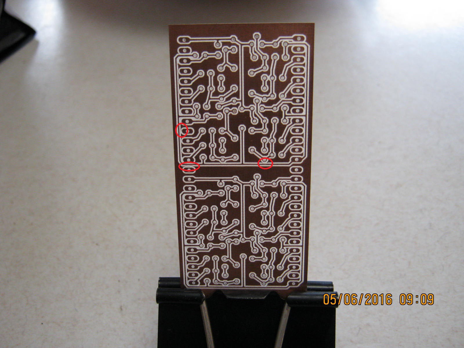
The initial results:
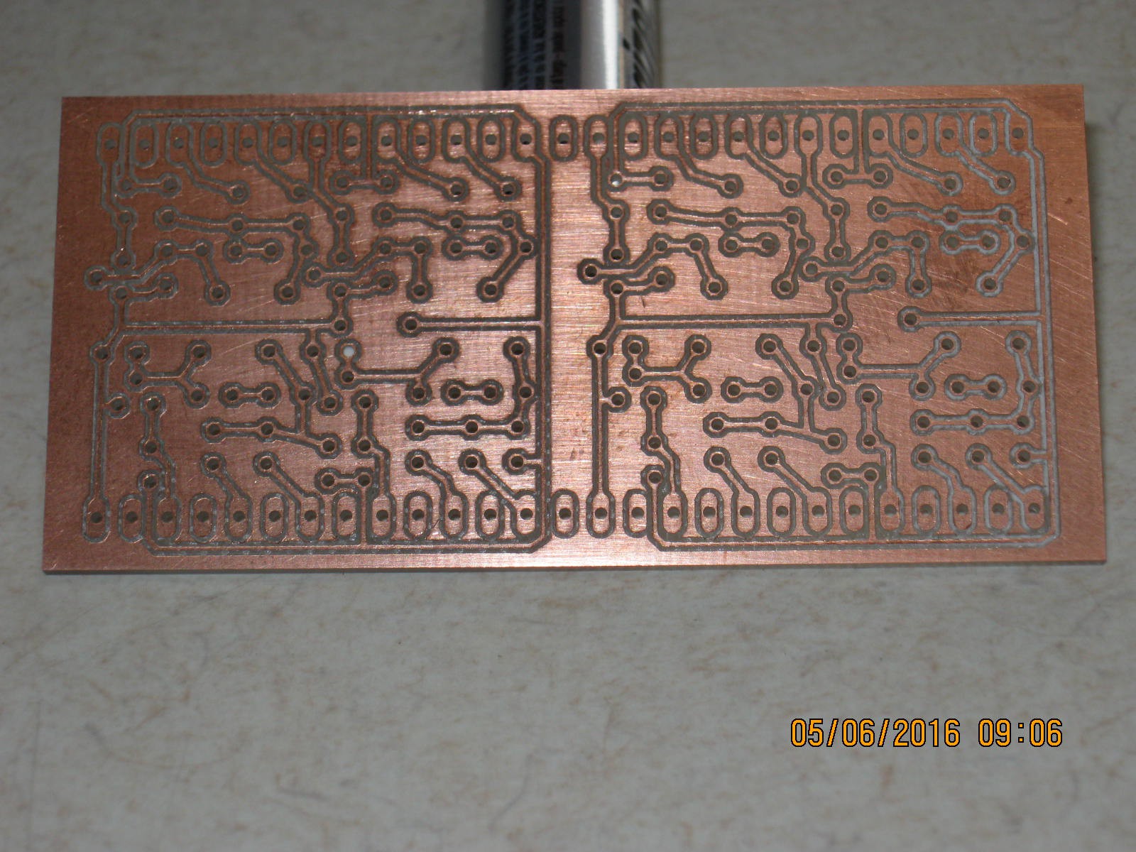
Problems with copper burrs.
Use a green scourer pad to remove:
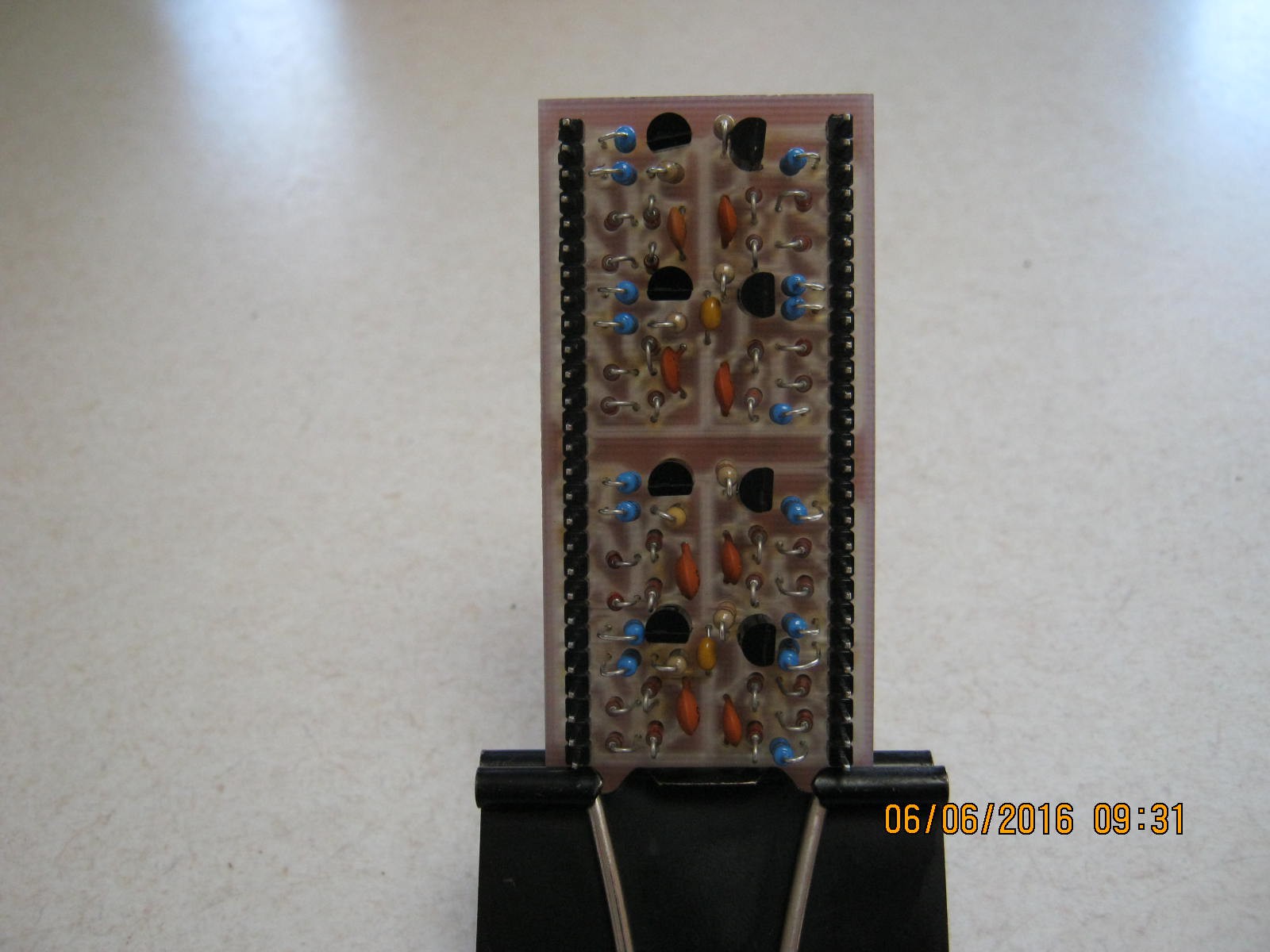
Completed project (top view):
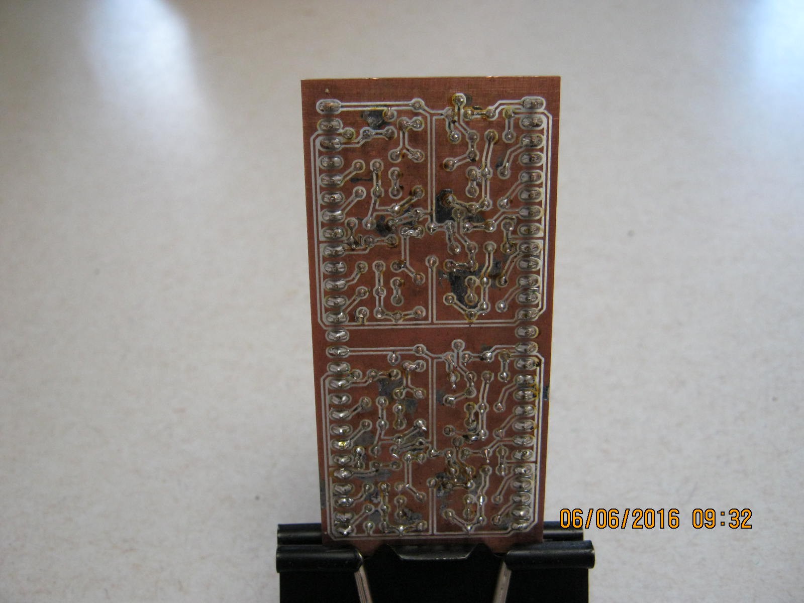
Complete project (bottom view).
My eyesight is not that great now, soldering for me is more like pushing the iron and solder in the general direction of the part and hoping for the best! My iron is 35 years old and has not shrunk to keep up with modern electronics. Still not too bad:
Ready for testing.
The main problem was that the isolation cut with was closer to 0.3 mm rather than 0.2 mm.
Therefore the copper tracks where reduced to 0.1 mm rather than 0.2 mm
Controlling the board height or cut depth to 0.1 mm needs more thought.
Perhaps two passes, one at 0.1 mm and them 0.2 mm if necessary.
But overall very happy with my first attempt.
Regards AlanX
 Jan B.
 martin.z
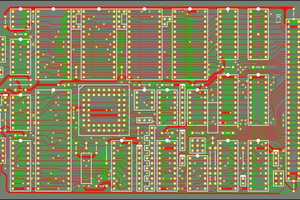
 Keith
Keith