 Erik Piehl
Update 2016-09-26: SD card access now works
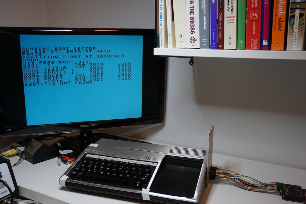
This is one of the first runs of my memory dumper "cartridge" reading data off SD card. The code reads the master boot record, then parses the partition table etc and finally reads and shows the contents of the root directory. This code only understands FAT16 partitions, and does not support yet SDHC cards, so it is running of a 2GB regular micro SD card.
Update 2016-09-24: GROMs moved to RAM
So far in this FPGA design I've kept the GROM memory contents stored on the FPGA's block RAMs, emulating ROMs. The ROM contents became initialised as the FPGA was initialised. But that did limit the amount of GROM the design could include and also made it slow to modify GROM contents. So now I set aside a one megabyte region for GROM contents, and using the PC USB loader I can initialise the GROM contents in the external memory.
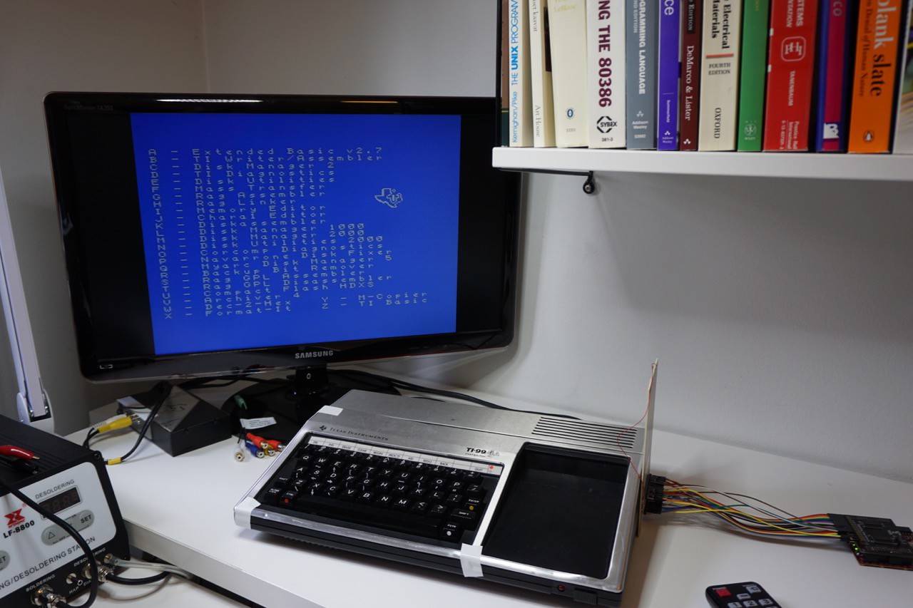
Below I have XB2.7 suite running on the TI console. This is usually done using a cartridge, housing 512K of ROM and 120K of GROM. Now both are being served by the FPGA - along with the memory extension.
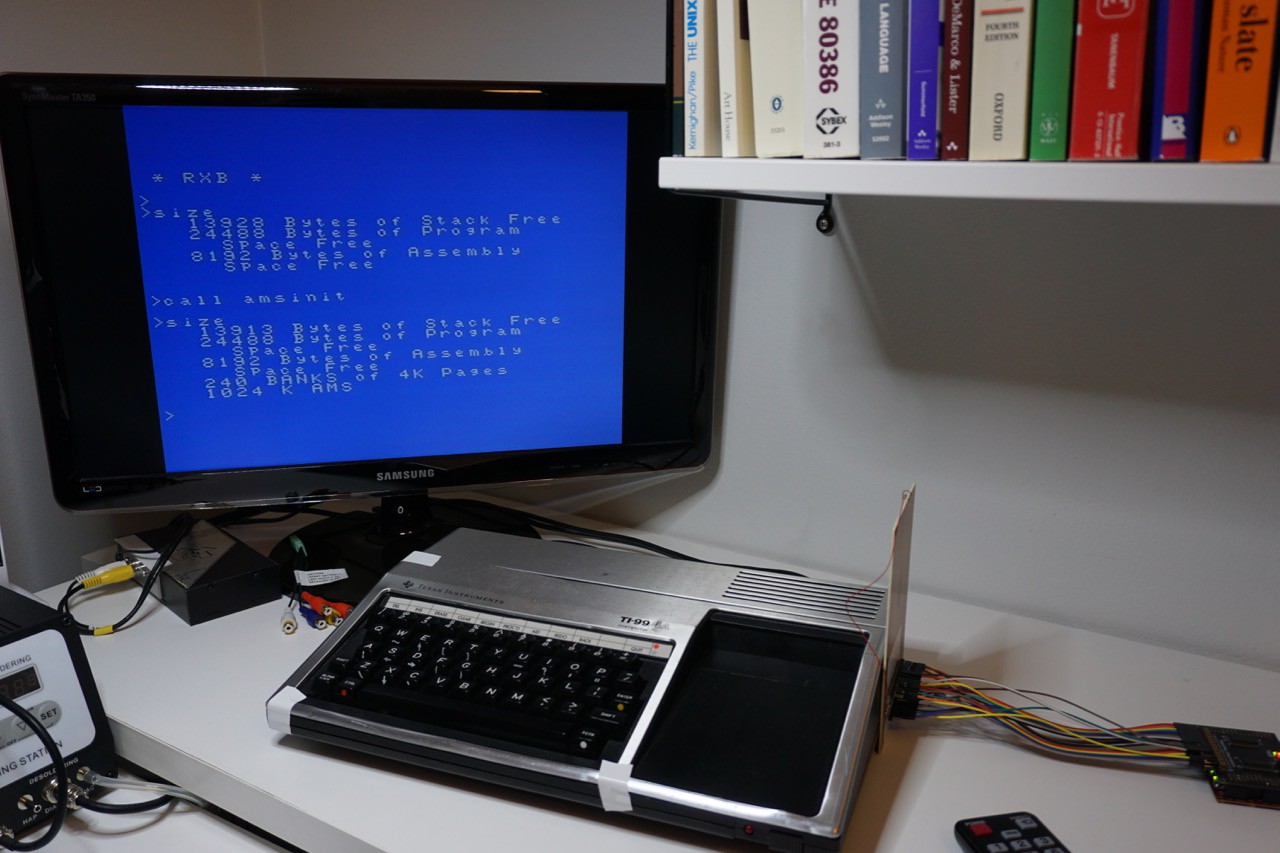
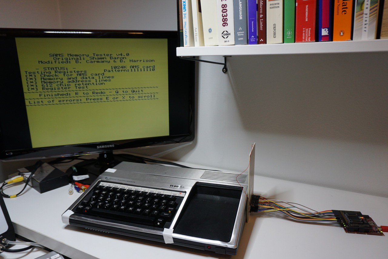
I also tested RXB2015 (another extended Basic), and that worked too. RXB supports SAMS memory, so it was great to see that being detected and working nicely.
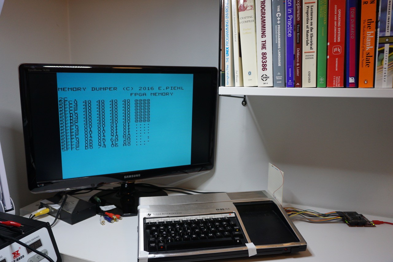
Update 2016-09-20: SPI interface and memory dumper
Now there is an SPI interface in place. I adopted it from an earlier design of mine. Testing the SPI requires some driver software, so I put together a simple program to dump memory as a starting point for the SPI testing code (the SPI drives the SD card interface). The memory dumper app includes code to display text on screen and keyboard processing, so the basic building blocks are there. The memory dumper program proved immediately useful, as I finally got the SDRAM interface robustly working. Since PC connectivity is already there, I utilised that for hardware debugging: pressing the period key in the memory dumper copies the values of some hardware registers to memory extension, allowing the PC memory reading capability to reach those values without having to modify the FPGA. The memory dumper itself is written in TMS9900 assembly language and runs in the cartridge memory space (address range 6000..7FFF).

Update 2016-09-04: PC connectivity
In a hobby project like this one, I usually want to build things in an incremental fashion, one small step at a time. So far the project has advanced pretty nicely by just going after the low hanging fruit - basically implementing more or less existing functionality in the FPGA (existing as in RAM extension, cartridge emulation etc.).
Sometimes the small steps just are not possible. For me it came with connectivity. I wanted to finally get to a phase where the modern world would meet the TI to the extent that I could push easily software into it. So I wanted to have PC connectivity - but not your average with a serial port. This project is running on a very high-performance FPGA, something better surely can be done?
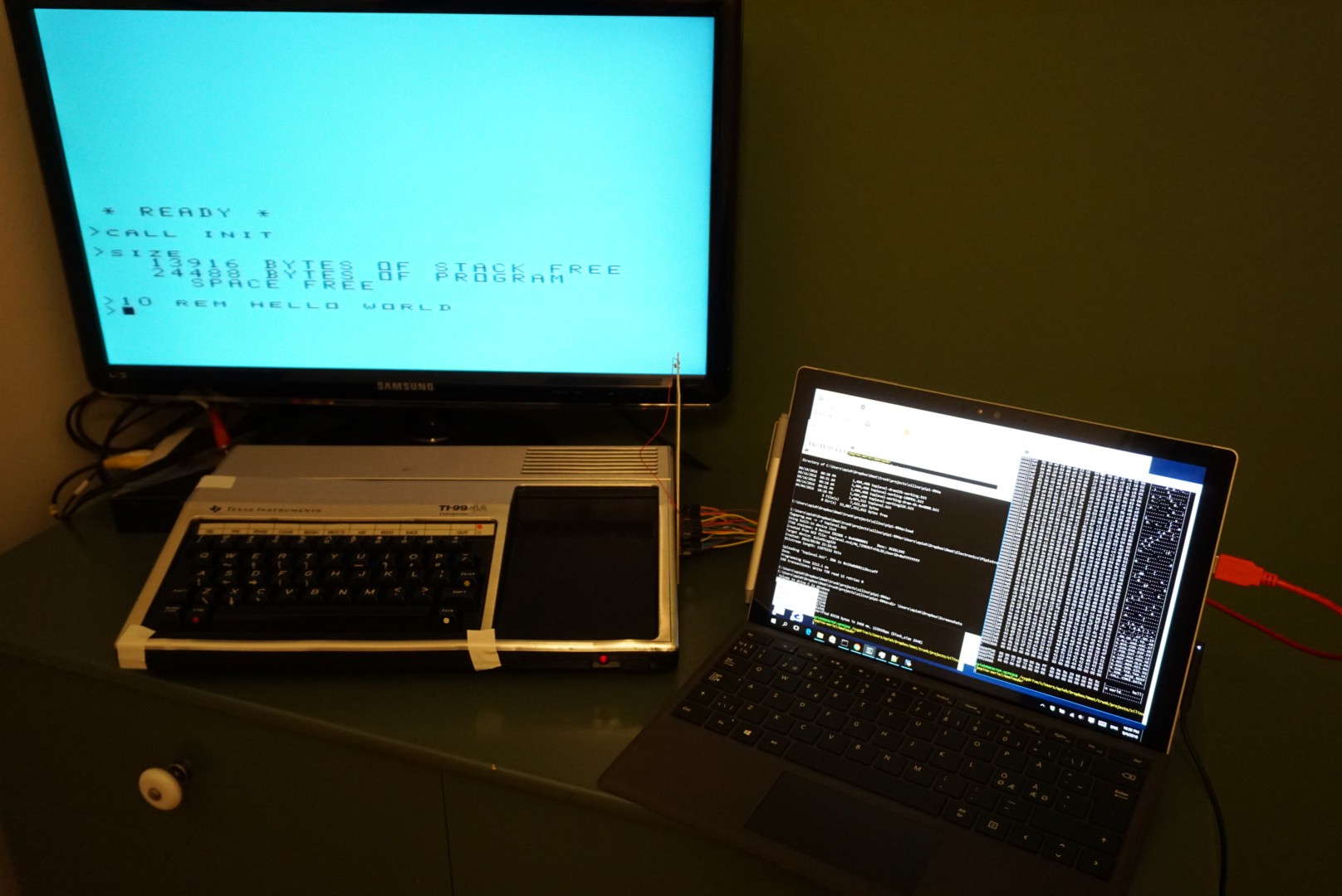
Well I got something much better done. I still have the UART for serial communication, implemented in the FPGA. But it is not the CPU of the TI-99/4A that is communicating with the UART. Instead, there is a hardwired state machine that provides PC access to the memory space concurrently to the TI, basically while the TI is running full speed there is sideband channel that allows a PC to issue commands using the serial port to read and write to memory, without the TI noticing. Serial communication is currently running at 230400 bps, but that could be pushed higher. In practice the serial traffic happens over USB thanks to the FTDI chip on the board.
Alas, that turned out to be more work than I perhaps expected. There were a whole bunch of things to work on, all which were pretty much necessary to complete this feature:
- Define a protocol that is simple enough for a simple state machine to understand, yet...

 SHAOS
SHAOS
 EtchedPixels
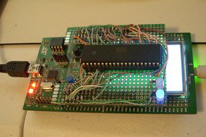
 Reed Foster
This really brings warm and fuzzy feelings as the TI 99/4a was my first computer. Did a lot of assembler programming back in the days. Also made an I/O card once but writing a good DSR was a bridge too far back then.