 [skaarj]
Data needs to be read fast and precious time is waisted with traditional approach:
- continuous reading of GPIO ports and wait for them to confirm the data is ready for pick-up;
- store the byte inside a variable;
- convert from IBM-style to normal style using either math or a lookup table (faster!), invert the byte
- append the byte to the end of a string;
- push each string to microSD card at every end-of-block;
- try to catch a new read and try not to lose data if all the above tasks together take more than 1.2 microseconds to finish.
All these operations waist precious time so special measures had to be taken:
1. Pertec works in inverted logic (0V means true, 5V means false). This allows for long cables and little noise influence but requires special attention at software level, so each buffer contains the Soviet Union equivalent of 74ALS640 / 74ALS642: the K555AP9. This inverts the received data - thus saving precious CPU time and also making the programming easier without any software inverted logic.
The "normal" circuits were tried first:
- non-inverting data output 74LS/ALS/HC/HCT/N/S-245, 74LS/ALS/HC/HCT/N/S-641,;
- inverting data output 74LS/ALS/HC/HCT/N/S-640 and 642, both normal and -1N variant (double miliamp output signal intensity)
All of them in SMD and THT variants.
Either I bought a lot of trashed parts from respectable, unquestionable great suppliers - which I seriously do not believe - or the soviets had a better design because the 'normal' (74-series) circuits caused surges in the power supply unit in bypass and service mode and they became extremely hot. At first I could not believe and I blamed the soviet chips for destroying my tape drives and my Pertec controllers. I developed a theory about black holes feeding on $$, explained later in this text.
Anyway - I saved a lot of CPU time by passing all byte-inverting operations to external circuitry.
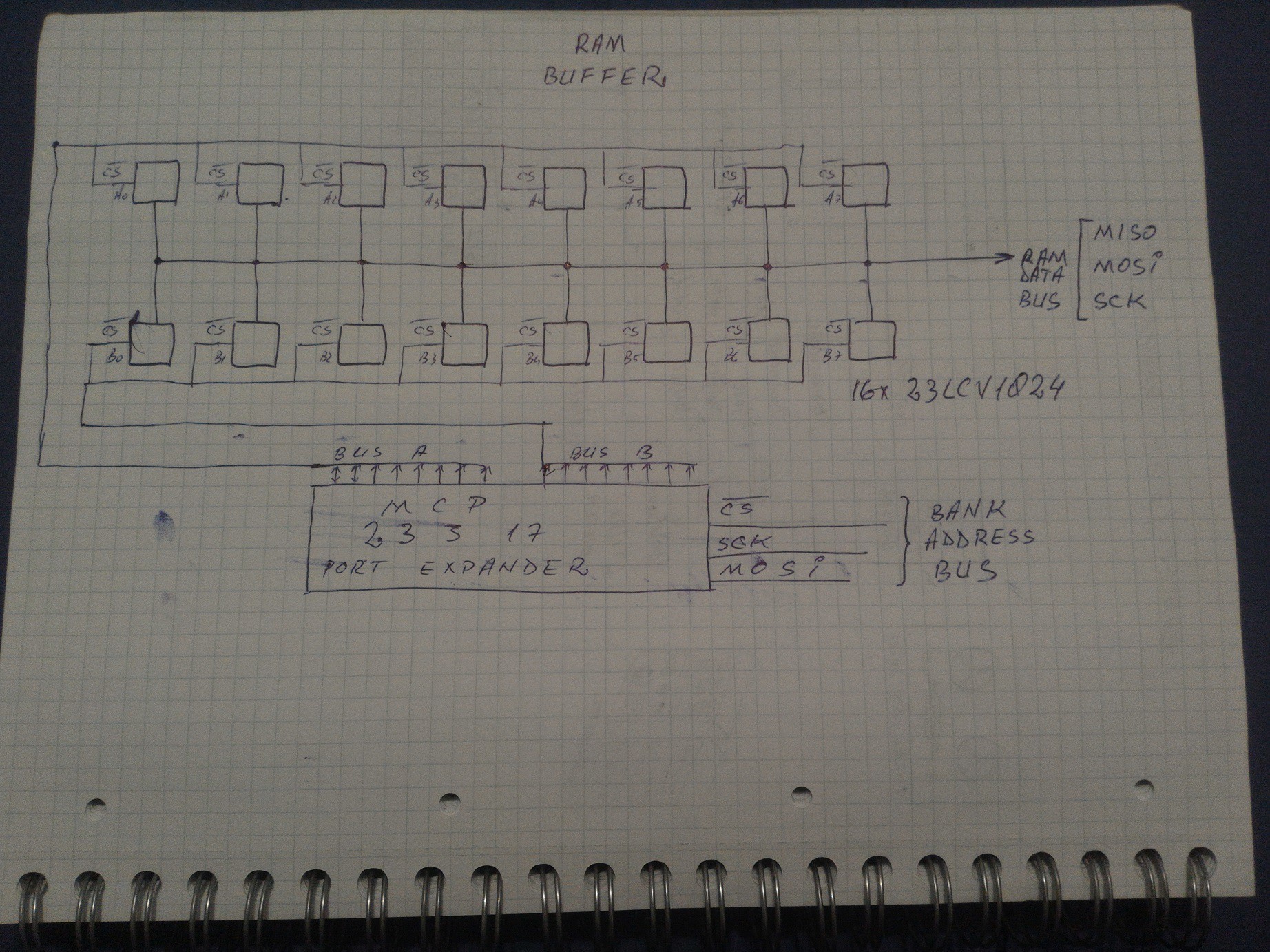
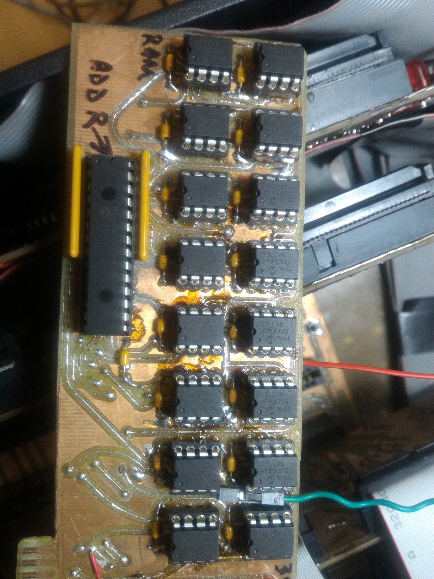
2. Build a fast ram bank using 16 x 23LCV1024 (128 kBytes) high speed serial SRAM.
As a note: I don't use commercial measurement units. They are lies and blasfemies for the technical part: a Megabit counts stuff to trick people. It is an advertising measurement unit which lies about how great is to see the data rate 8 times bigger, larger and faster than the reality.
A Megabit is some kind of eye drops Viagra: you drop it in the eyes and see things eight times bigger.
A megaByte represents a quantity useful in computing and it is 1/8 of a megaviag..bit. The French are wise - they say "mega-octet" to avoid tricking people and I respect them for that.
So 23LVC1024 holds 128 kBytes - the great "Megabit" which represents around 9% of a 3.5", 1.44MB floppy disk.
Using 16 of them I built a 2 MBytes RAM bank with custom addressing control.
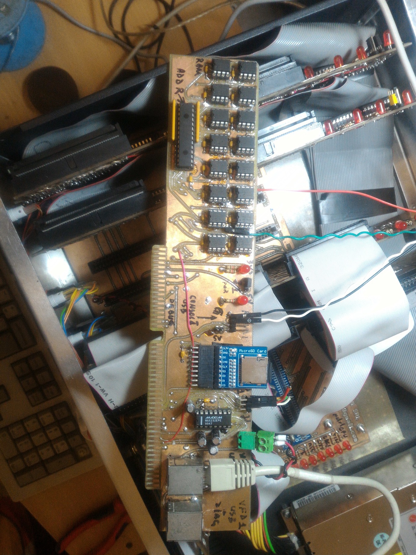
This is the system RAM buffer + uSD storage + serial communication.
The addressing is performed via one MCP23S17 SPI Port Expander from Microchip, thus saving 13 i/o pins on the controller side: 16 chip-select + 3 SPI without the PEX, only 6 SPI pins with the PEX. More RAM, more port expanders (PEX). If a lot of RAM, the addressing expanders can be.... selected using another PEX. Or a FPGA logic approach which saves a lot of space, time and speed. It's starting to sound like some $$-absorbing black hole theory.
3. I also defined two DMA stream channels to get the fastest speed available for these 23LCV1024 - actually they should be called 23LCV128kB - circuits according to their datasheet. However the addressing control do not support DMA so this slow things down for a bit. Not megabit.
4. Interrupt requests. A design flaw in the schematics turned to be tricky at software level because in STM32F429 microcontroller, the External Interrupts 9->15 treat all GPIO pins 9...15 from all the ports at the same time and it is not possible to set different priorities for each pin. It may be required to rebuild the motherboard as it is already cut and patched in many places due to the CNC faults.
When performing tape i/o data operations, the ram buffer is used and the corresponding DMA channel is activated for either Tx or Rx data.
__________________________
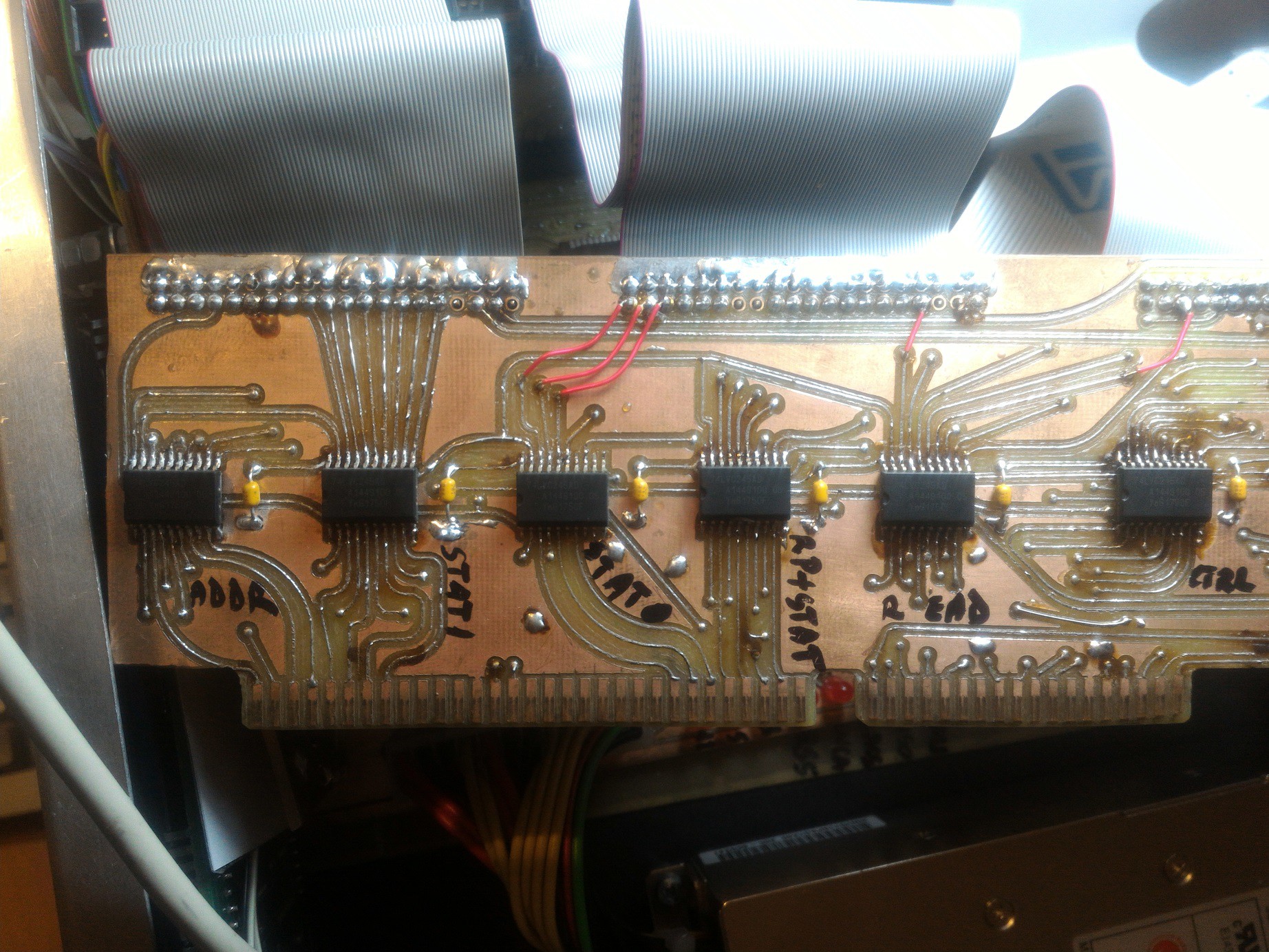
Level shifting, bidirectional i/o data buffer for the STM32F4 microcontroller
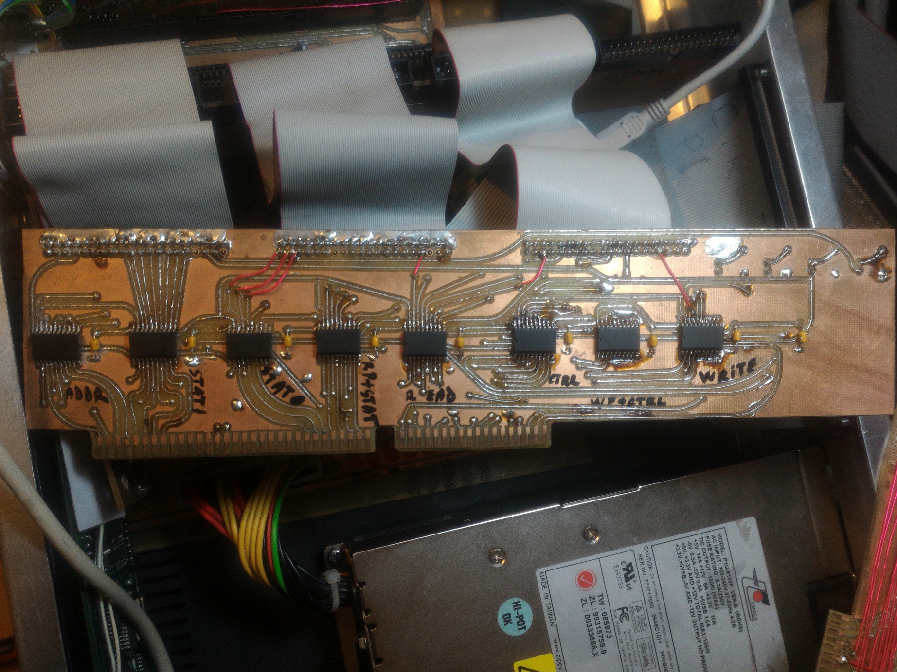
From write to left, first failed experimental buffer built with 74LVC245AD - 5V tollerant, 3.3V powered SMD, now working with 555AP9 (military grade):
Write, Write Parity + Control, Control, Read, Read Parity + Status, Status 0, Status 1, Addressing.
All the groups are defined in the code section inside the previous log.
[END OF TRANSMISSION]
Discussions
Become a Hackaday.io Member
Create an account to leave a comment. Already have an account? Log In.