 Yann Guidon / YGDES
Here, I'm scratching a "proto-computing" itch that is rooted in the 50s and 60s, as explained on Wikipedia:

Another version (with significantly different resistor values) found at http://digitalbyte.weebly.com/logic-families.html
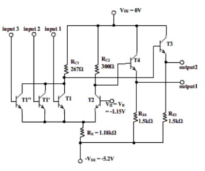
Here, silicon NPN transistors are used but ECL was invented around 1955, when silicon transistors were not really working (and PNP was the king). This means that there must have been ECL circuits with Germanium PNPs.
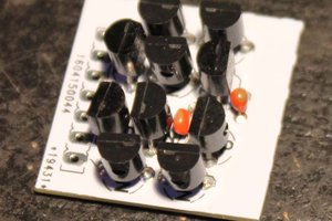
Back to 2016: my friends here play with discrete transistors, mostly with DTL circuits: #AYTABTU - Discrete Computer, #The T-1: A discrete 8-bit Stack Computer or #Germanium Calculus use pull-up resistors and reach a few MHz.
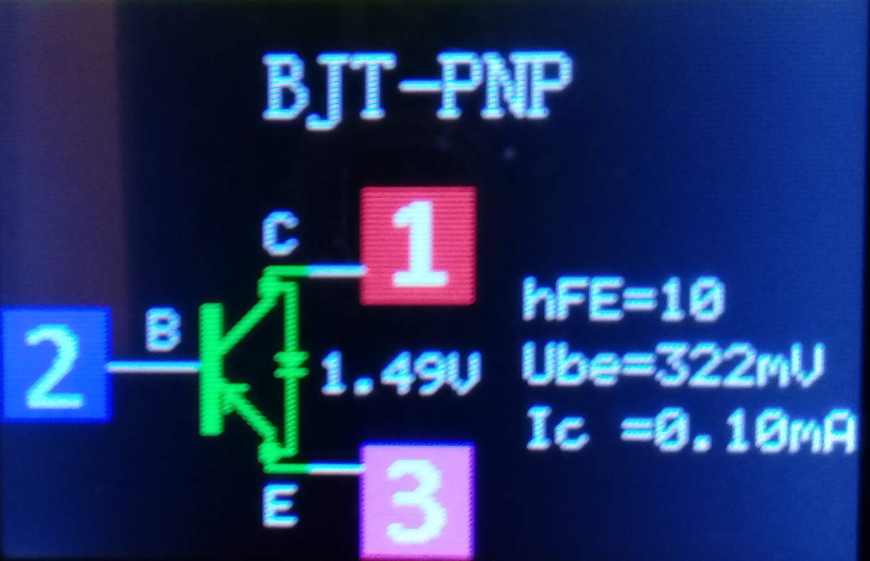
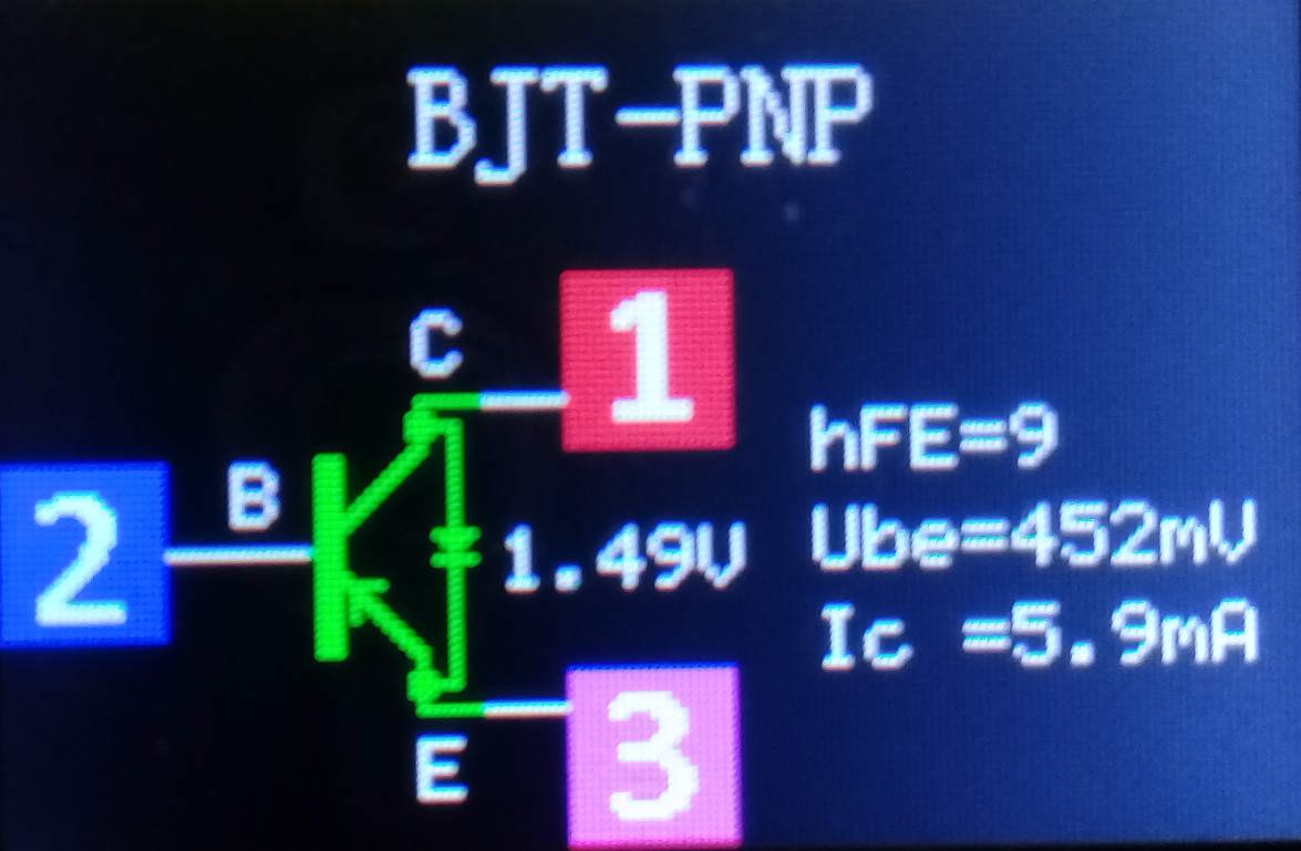
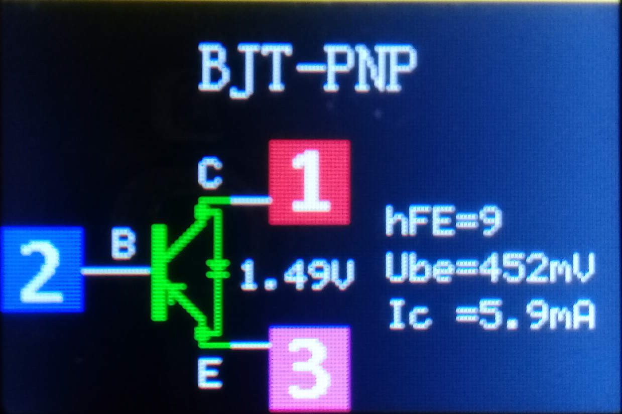
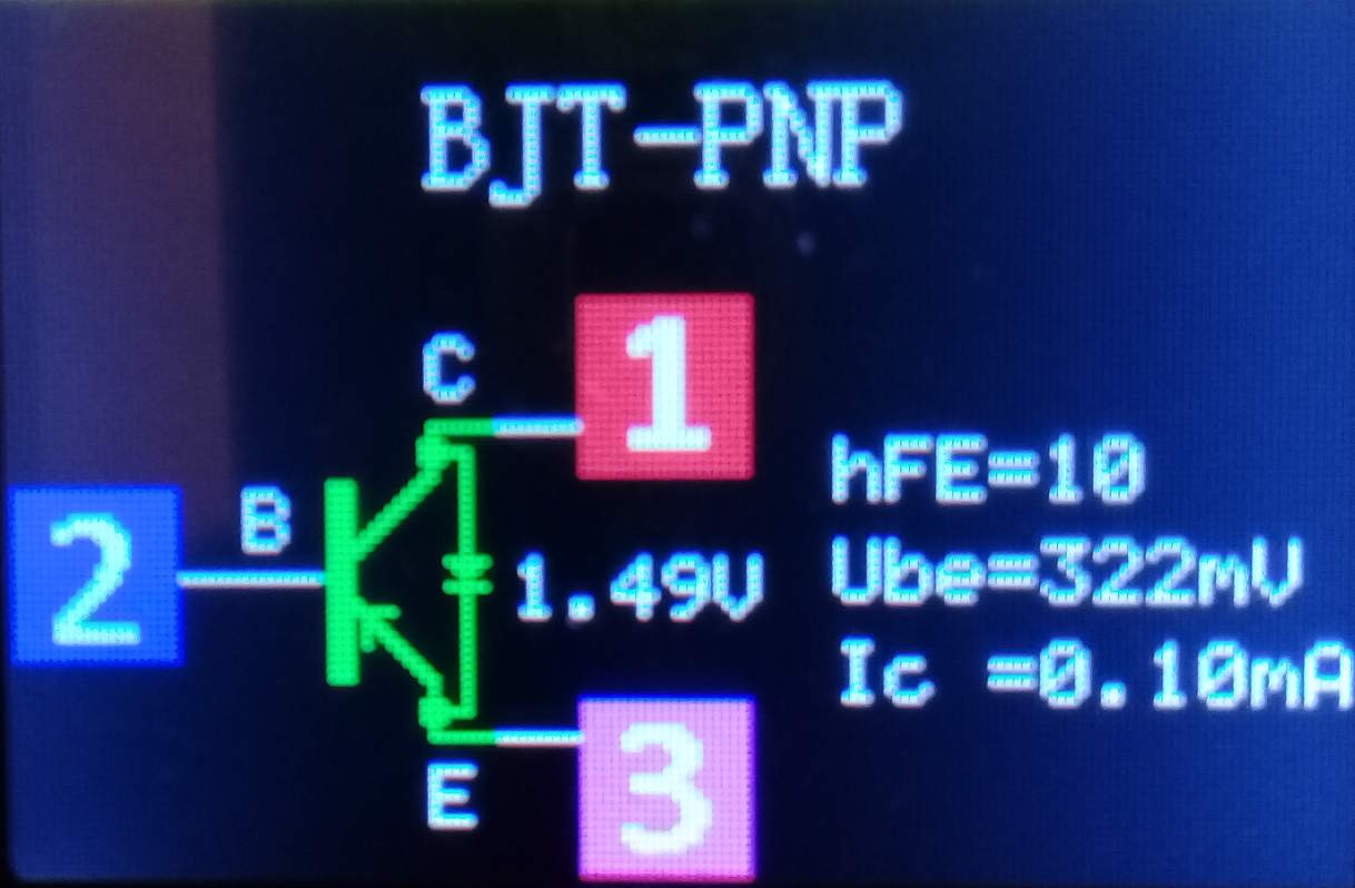
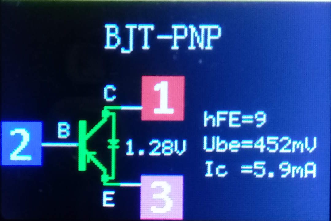
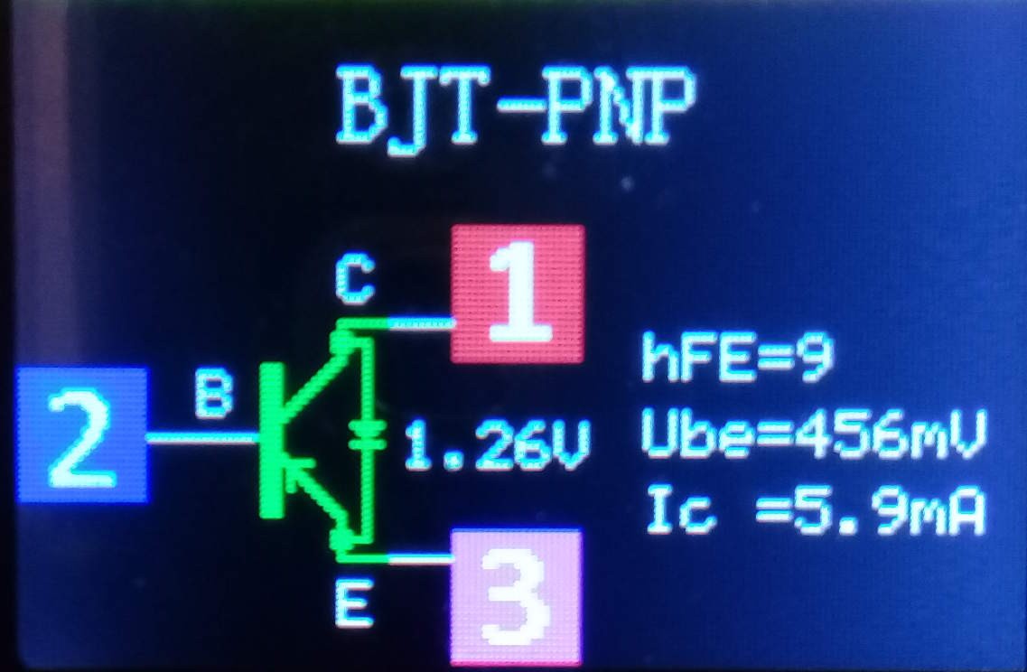
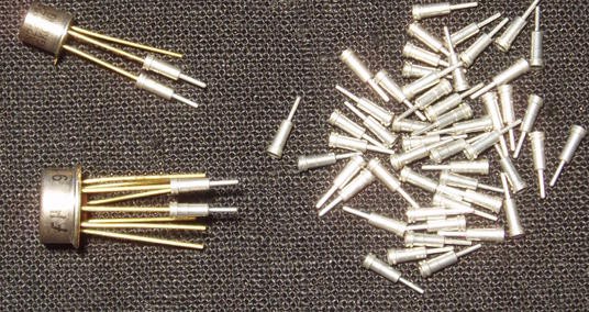
Now, I have come across a supply of PNP germanium transistors, mostly for analog and radio applications:
- AF138 (25V hFE=60...100, 60mW 40MHz)
- AF200 (25V 10mA 225mW hFE>30, PNP germanium mesa transistor intended as TV IF amplifier, 1963-1965, freq. varies depending on the sources: 35? 100? 200?)
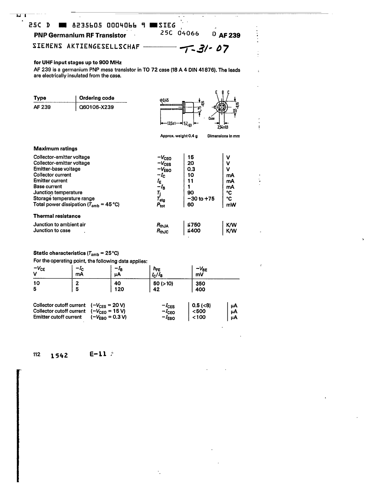
- AF240 (15V, 10mA, hFE=25, 60mW) reaches 500MHz (at unity gain)
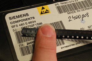
- (see Inventory #2 )
I also have some AF178 (180MHz, PHILIPS) AF137 and G106T (β around 60, 35MHz) but not enough to make something significant. The AF138 will do the bulk of the processing with some help from the others.
With >35MHz transistors, it must be possible to create pretty fast gates, no ?
From https://en.wikipedia.org/wiki/IBM_7090#Transistors_and_circuitry :
The 7090 used germanium alloy-junction transistors and (faster) germanium diffused junction[5] drift transistors. More than 50,000 in all.[6]
The 7090 used the Standard Modular System (SMS) cards using current-mode logic[7] some using diffused junction drift transistors.[5]
so YES there was ECL with advanced Germanium ! "Drift" technology was one of the last before Silicon took over (and powered CDC's 400K-transistors behemoth)
Update:
- I got a new oscilloscope (4×300MHz, the beloved 2465) and a 11302A (advertised as capable of 4×500MHz).
- I found a DDS that can reach 200MHz (stable level up to 70MHz)
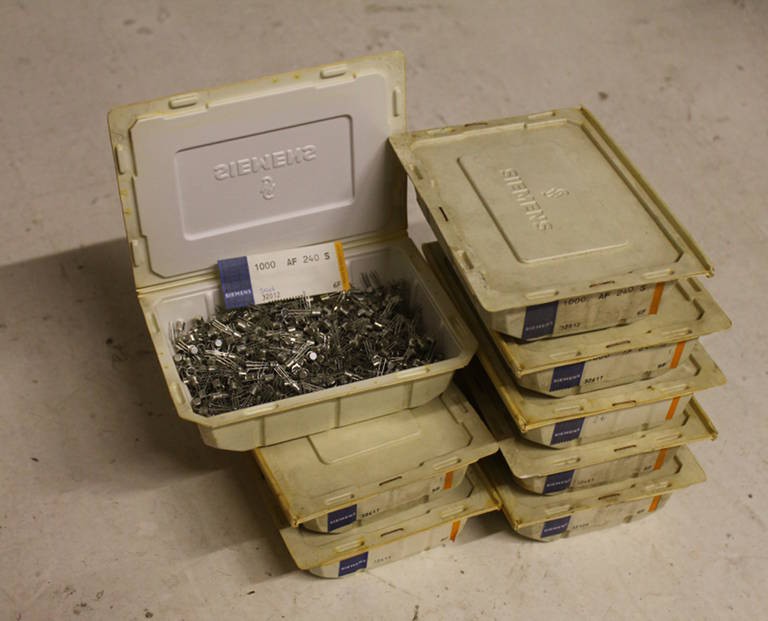
- I also found more AF240S...
This means I won't be limited by the AF138's low speeds !
Logs:
1. Inventory
2. Starting to "get" ECL
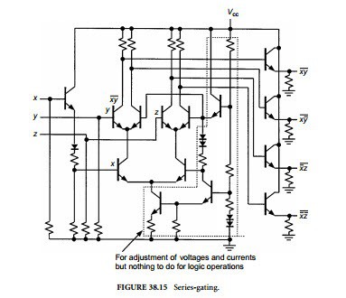
3. If in doubt, try to investigate how Seymour Cray would have solved the problem.
4. Inventory #2
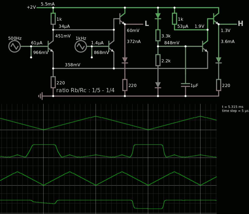
5. Fastest Germanium ?
6. The "language" of ECL
7. Register set musings...
8. More ECL musings
9. Advice from a germanium specialist
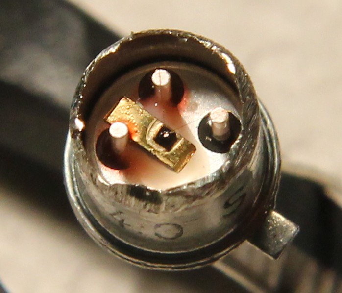
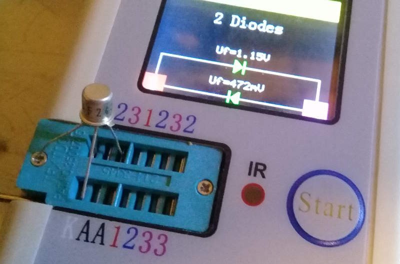
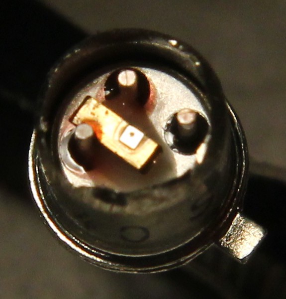
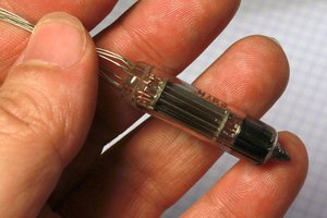
10. Inside the mesa can...
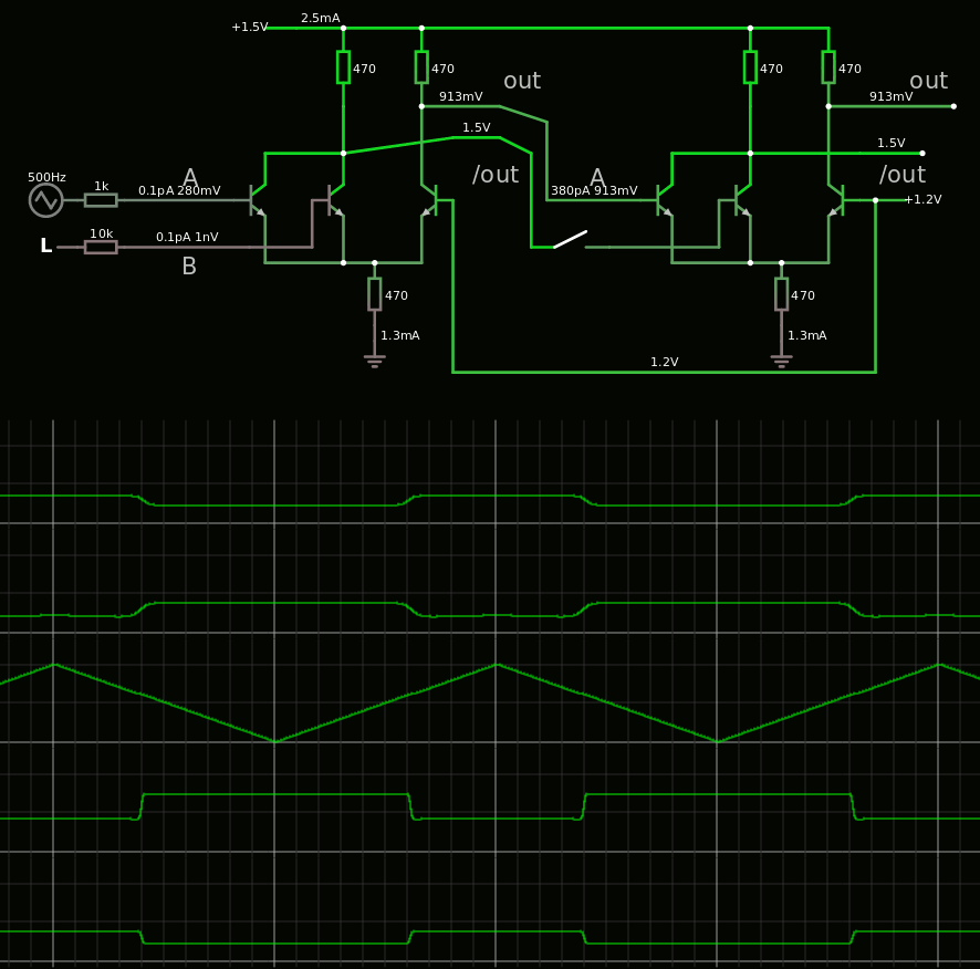
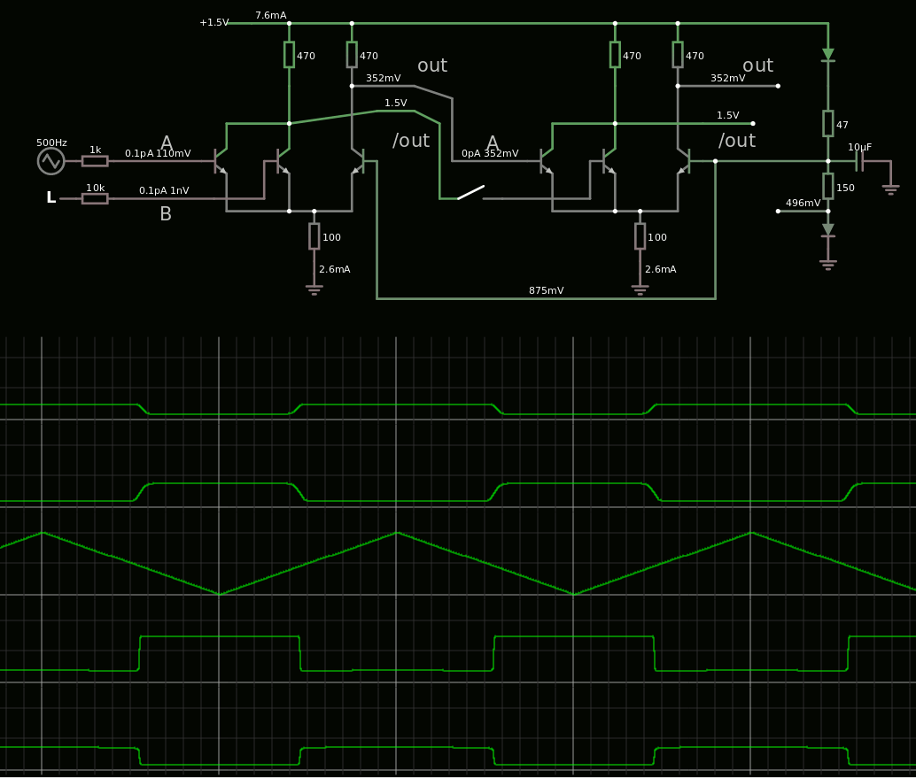
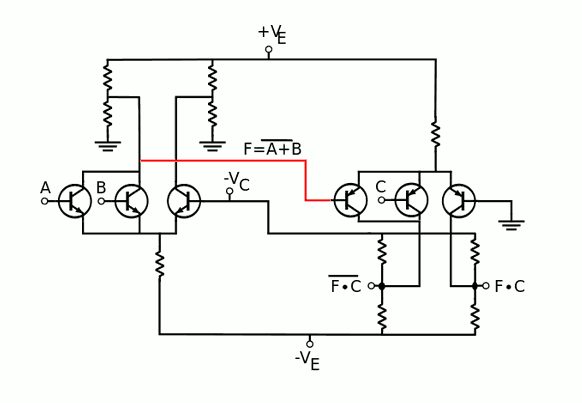
11. Complementary ECL
12. ECL is not dead
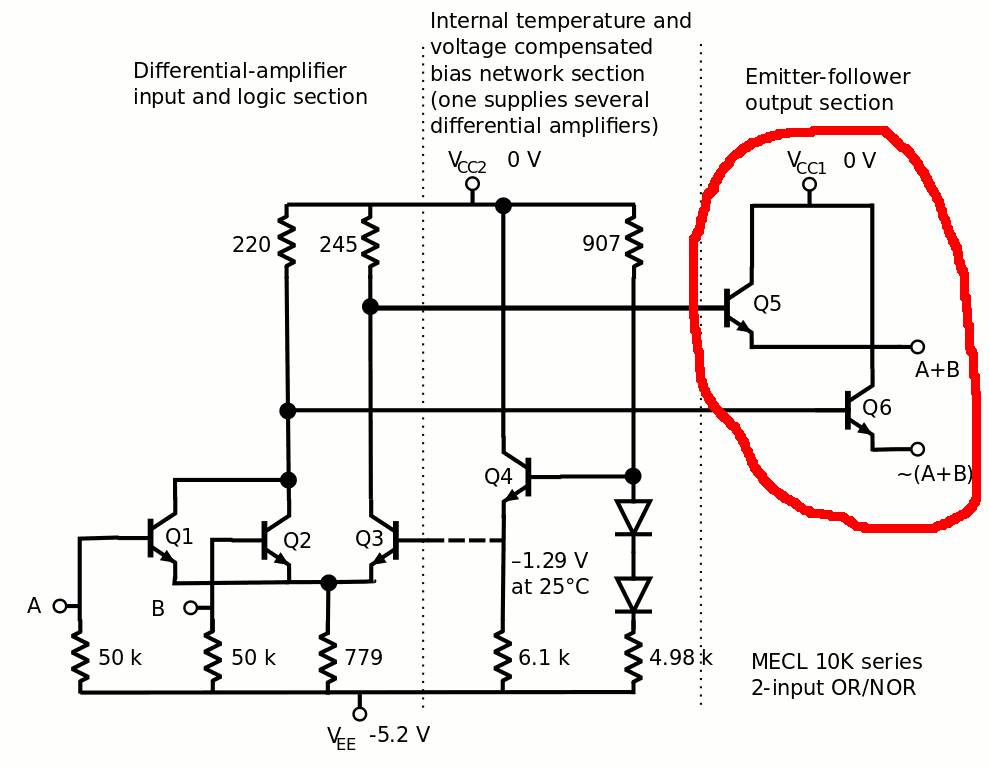
13. ABC of ECL
14. More complementary ECL
15. Low-Voltage ECL : part 1
16. Low-Voltage ECL : part 2, Current sinks : here we go again !
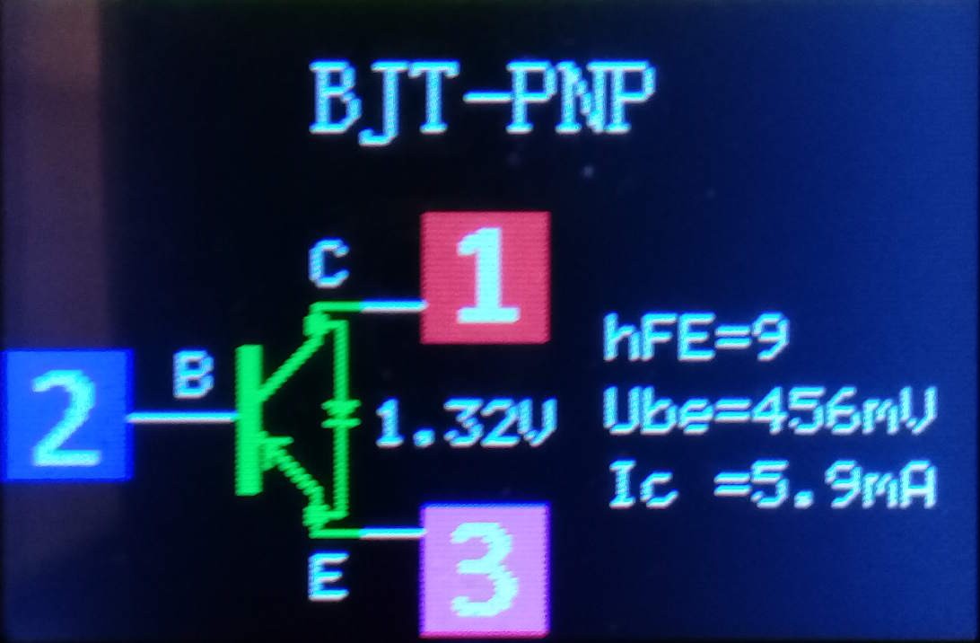
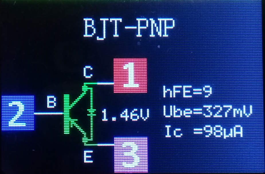
17. Testing the AF240
18. More characterisation
.


https://archive.org/details/High-speedSwitchingHandbook