 Yann Guidon / YGDES
This project was not initially meant to become a high-performance processor, but a generic tile, like the am2900 bitslice or the 74LS181 chips.
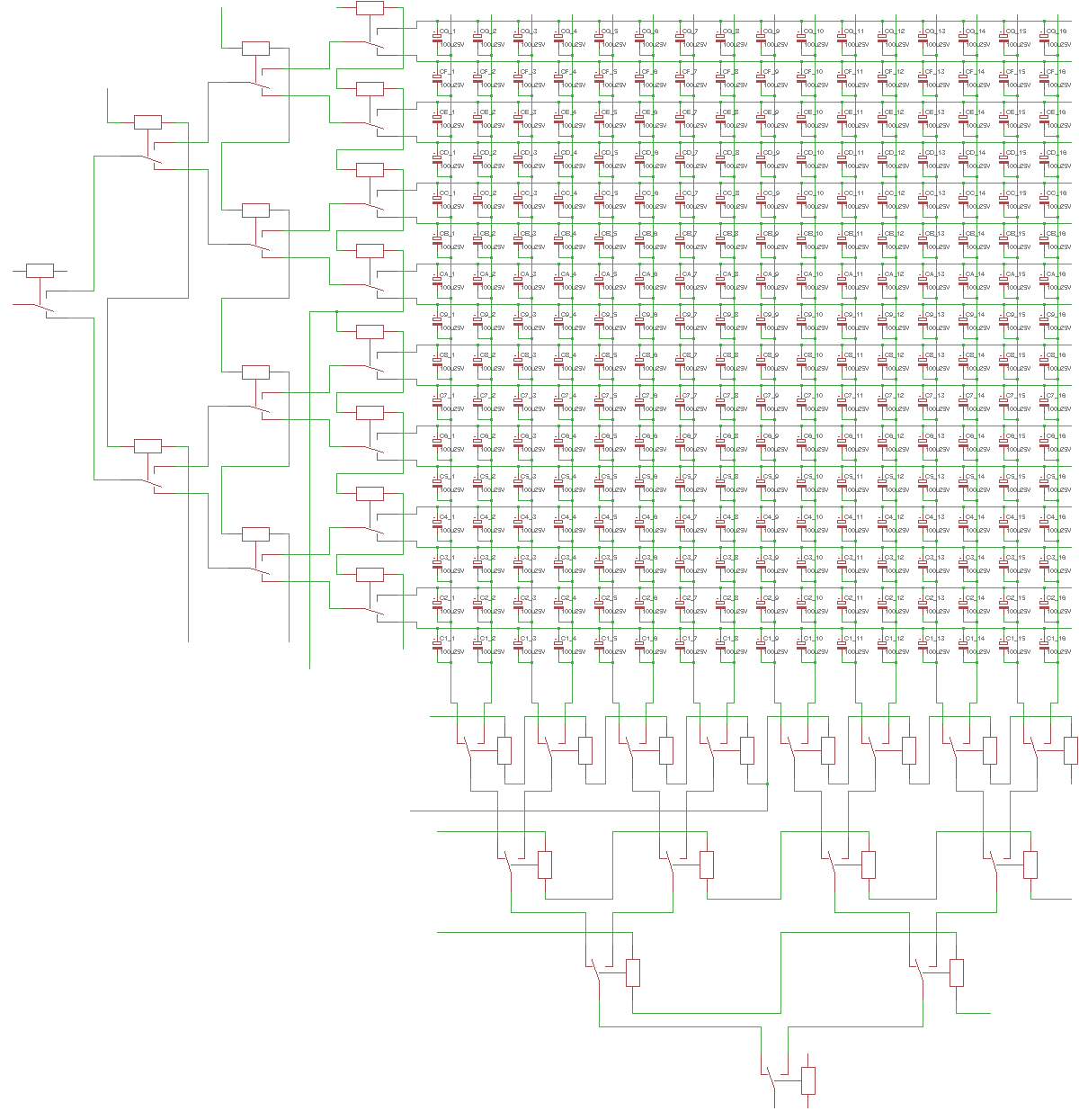
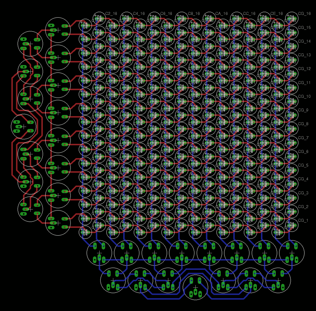
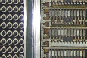
The difference, though, is that this slice is really one bit wide and each slice/module includes the necessary registers. Actually, it's an extension of the #SPDT16: 16-bits arithmetic unit with relays datapath, with logic functions added, and more registers.
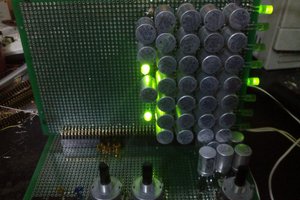
The first implementation is with relays : #YGREC16 - YG's 16bits Relay Electronic Computer (moved to #YGREC-РЭС15-bis)
Faster versions with Germanium, Silicium and CMOS are in the works, and other technologies should appear later. For example, it's also a good candidate for an ASIC implementation :-)
A smaller core, the byte-wide #YGREC8 might even be the first to become operational in FPGA then with #Shared Silicon...
The "AMBAP" principles are the heart of the YGREC microcontroller family and the foundation for the redesign of #F-CPU. The #YASEP Yet Another Small Embedded Processor already pioneered many of these ideas.
This is the result of a thought experiment : as I wanted to design discrete computers with various technologies, it was hard to estimate how many gates, transistors, relays, or parts, would be required. How many elements should I buy to reach a given level of functionality ? If I can acquire X parts, what am I able to build and what will be the performance ? What will be the datapath width, instruction set and capacity ?
Dieter went through the same thought process before me: "Second: It turned out to be hard to estimate the size of the CPU (or the number of transistors)." so he built a TTL machine...
The solution I found is a set of recipes :
- Forget about the instruction set. It's a distraction. First, design the computing elements then wrap them around suitable control logic when the computational datapath is ready. Good old RISC principles will do the rest. Like, keep everything dumb, orthogonal and 1-cycle.
- Only include the vital circuits to perform Add/sub-related instructions, ROP2 and some shift. Keep the critical datapath short and simple. Multiplies, division, barrel shifter and anything else belong to external, slower units (with potential for pipelining).
- You basically need to care about the following fundamental circuits : MUX (MUX2, MUX4, MUX8), XOR, latch and/or DFF.
Actually, once you have a MUX, you're almost done since you can do everything with a MUX ! - Focus on only one bit of computation and make it a tile that you can copy-paste at will. This way, you have a rough formula, depending on the number of registers and datapath width, that helps you tune your computer's size. It will appear quickly that 8 or 16 registers is a "sweet spot" but it can be changed at will.
- Register-mapped memory increases the number of necessary registers but saves a lot of complexity. It also makes the architecture more scalable and increases performance, with simultaneous accesses from separate arrays. I've solved the fundamental issues with the #YASEP Yet Another Small Embedded Processor so go for it. You can mix&match the configuration of the memory blocks according to your needs.
- PC as a general purpose register : usually required for general-purpose computing, you can keep it separate for special architectures (this saves one register, particularly if register addressing space is constrained). OTOH, a unified register file saves opcodes. So the rule of thumb is : PC is a user-visible register for 16 registers or more.
- Don't let yourself get caught in a nightmarish forest of control signals : it's nice to predecode as much as possible but high fanout signals can make the design impractical ! Find a compromise between local and global decoding. This varies from technology to technology...
Once you have good estimates of the complexity of each gate and circuit, you can estimate the cost/complexity/size of the bitslice and tune the parameters.
Logs:...
Read more »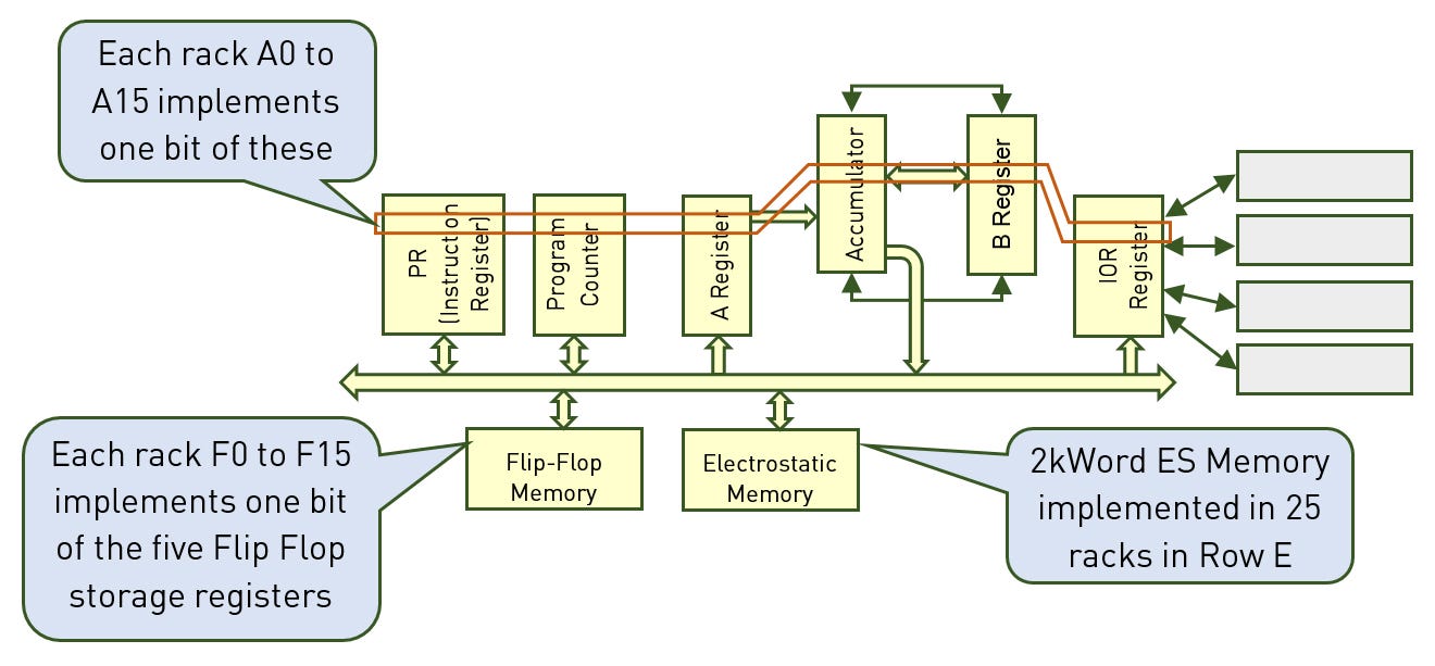
 There are:


 Stefano
Very interesting project - I have a similar one in early stages in my papers, it was to be a 1-bit slice using GAL22V10. 8 internal registers feeding through 2 parallel 8-to-1 MUXs into a 8 operation ALU (which is a 8-to-1 MUX, some selections implement left and right shift, and pass through of external data inputs). Write back to "regs" is implemented as a 2-to-1 MUX in front of the D input. Select of these is connected to to a 3-to-8 decoder with enable. This way in one cycle 2 independent values can be read and written into third (3 address architecture)