 agp.cooper
Debugging
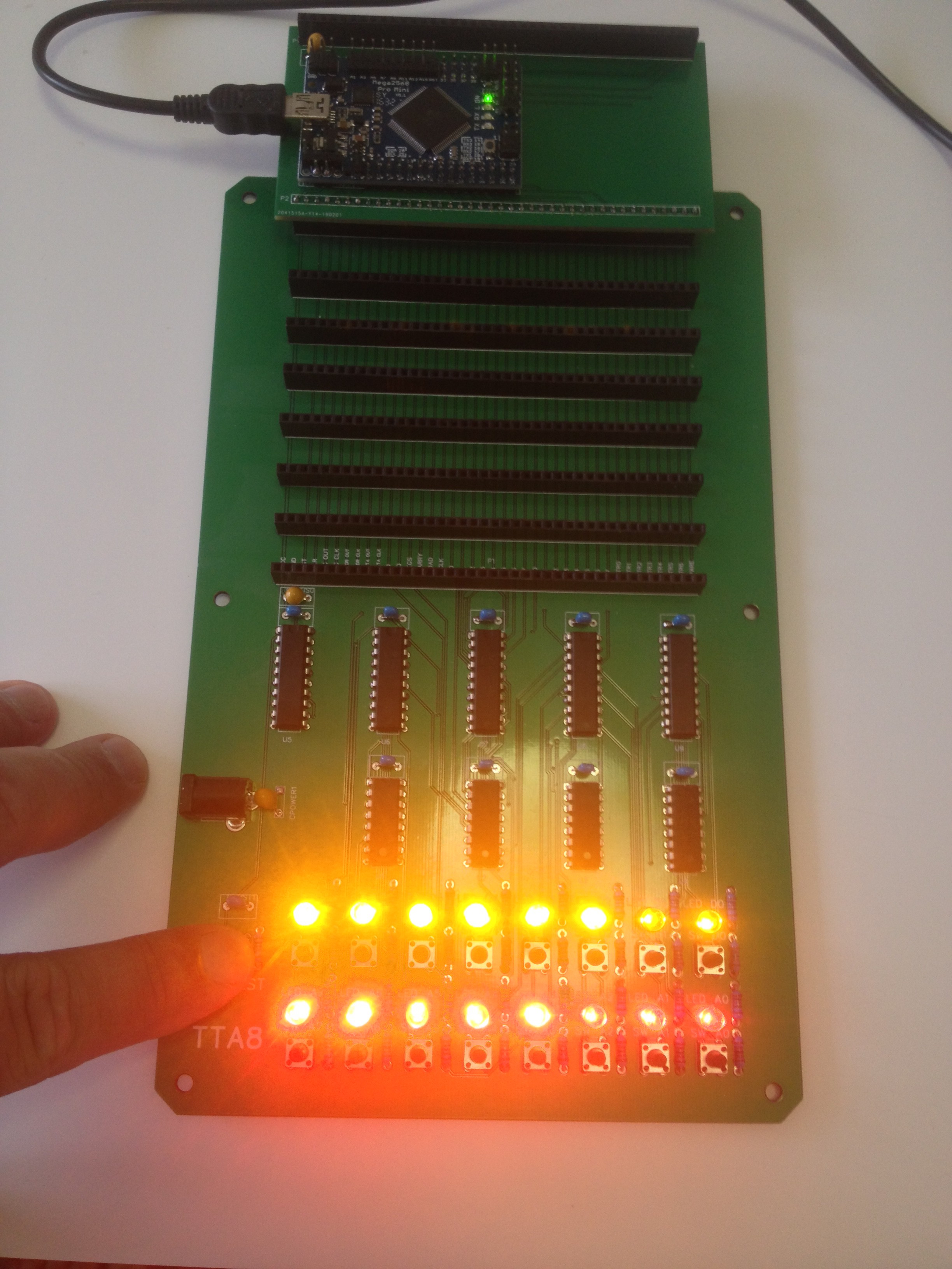
Need to get this project working.
One problem is that the Nano does not have enough pins.
So I have used a Meduino (a Mega2560 Pro Mini).
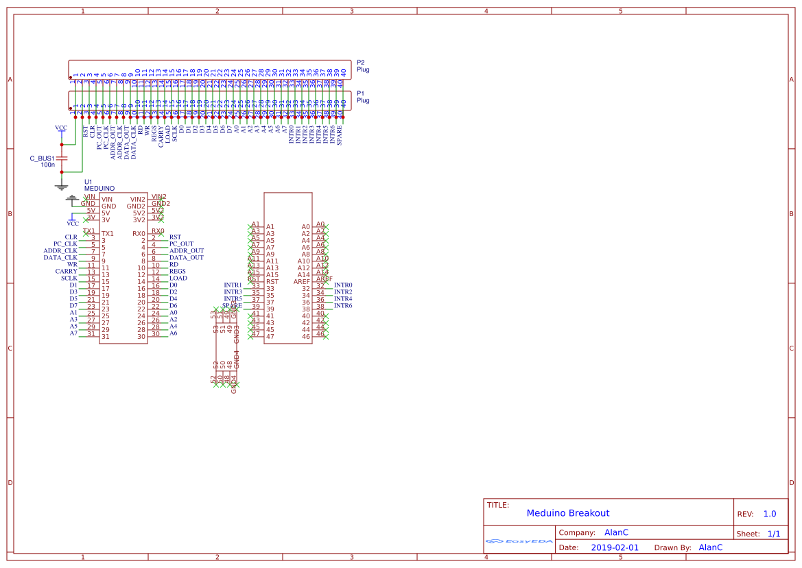
Here is the schematic:
Here is the PCB:
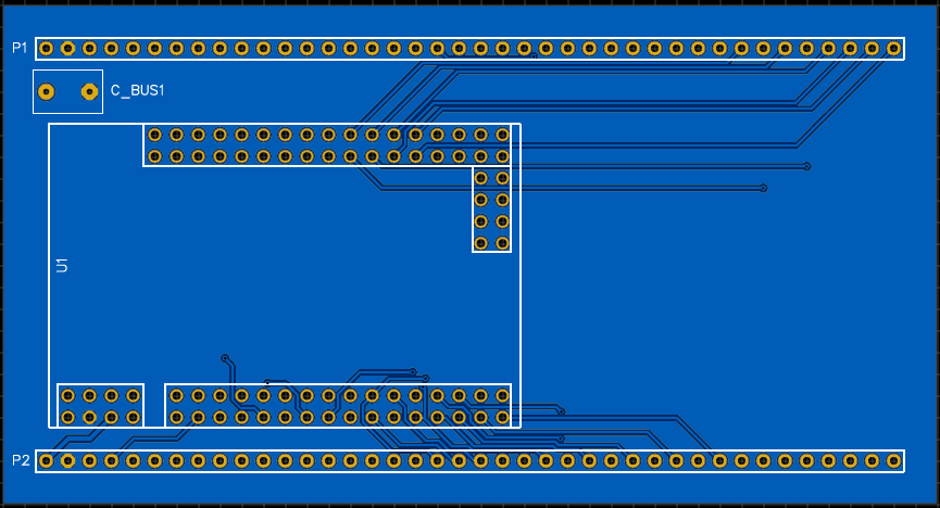
The ports (P1 & P2) match the TTA8 bus.
A problem with the Meduino is that pins do not align with the ports (unlike the Nano).
So it is awkward to go fast. Awkward just means more coding. But do I really need to go fast? This time I have coded using pinMode, digitalRead and digitalWrite.
Here is the Mother Board I/O test code:
/*
  Front Panel Board Test
  ======================
REGISTERS:
  Hex  Address Write   Read      Comment
  FF   255     JMP     INTR      Jump/Intr
  FE   254     JC      Reserved  Jump on Carry
  FD   253     ROM     Reserved  ROM PAGE
  FC   252     RAM     Reserved  RAM PAGE
  FB   251     REGD    REGD      DATA REG
  FA   250     REGA    REGA      DATA REG ADDR
  F9   249     REGQ    NAND      ALU
  F8   248     REGP    ADD       ALU

SYSTEM (Pointer to Pointer Copy):
  Hex  Address Write   Read      Comment
  F7   247     JUMP    JUMP
  F6   246     POINTER POINTER
  F5   245     DEPOSIT DEPOSIT
  F4   244     FETCH   FETCH
  F3   243     DATA    DATA
  F2   242     ADDR    ADDR
  F1   241     RETURN  RETURN
  F0   240     PAGE    PAGE

CPU MODEL:
  Hex  Address Write   Read      Comment
  EF   239     TEMP    TEMP
  EE   238     DELAY   DELAY
  ED   237     INTR    INTR
  EC   236     MASK    MASK
  EB   235     PP      PP        Page Pointer
  EA   234     IP      IP        Instruction Pointer
  E9   233     SP      SP        Return Stack Pointer
  E8   232     DX      DX        (Monitor Data I/O)
  E7   231     CX      CX        (Monitor Addr I/O)
  E6   230     BX      BX
  E5   229     AX      AX
  E4   228     TX      TX        Temp Register
  E3   STACK
  E2   STACK
  E1   STACK
  E0   STACK
  ...

  0xF8-0xFF REGISTERS  (8 registers)
  0xC0-0xF7 STATIC RAM (56 bytes at page 0xFF)
  0x80-0xBF PAGED RAM  (64 bytes)
  0x00-0x7F PAGED ROM  (128 bytes)

  CPU Emulation:
    This CPU has no actual opcodes.
    All instructions are MOVE from [PC] to [PC+1]
    i.e. Move DATA from source ADDRess to destination ADDRess.

    The 4 cycles are:
    1 Fetch the destination ADDRess pointed to by the program counter and put in the ADDR register
    2 Fetch destination DATA pointed to by the ADDR register and put and the DATA register
    2A  Increment the program counter (PC)
    3 Fetch destination ADDRess pointed to by the program counter and put in the ADDR register
    4 Deposit the DATA register into the destination pointed to by the ADDR register
    4A  Increment the program counter (PC)

    All hardware (PC,IO and ALU) is memory mapped.
*/

// Board Connections:
//       Bus       Meduino Pin
//       VCC
//       GND       Gnd
#define  RST       2
#define  CLR       3
#define  PC_OUT    4
#define  PC_CLK    5
#define  ADDR_OUT  6
#define  ADDR_CLK  7
#define  DATA_OUT  8
#define  DATA_CLK  9
#define  RD        10
#define  WR        11
#define  REGS      12
#define  CARRY     13
#define  LOAD      14
#define  SCLK      15
#define  Data0     16
#define  Data1     17
#define  Data2     18
#define  Data3     19
#define  Data4     20
#define  Data5     21
#define  Data6     22
#define  Data7     23
#define  Addr0     24
#define  Addr1     25
#define  Addr2     26
#define  Addr3     27
#define  Addr4     28
#define  Addr5     29
#define  Addr6     30
#define  Addr7     31
#define  Intr0     32
#define  Intr1     33
#define  Intr2     34
#define  Intr3     35
#define  Intr4     36
#define  Intr5     37
#define  Intr6     38
#define  Spare     39

void InitialiseBoard(void)
{ // Reset State
  pinMode(RST,INPUT_PULLUP);   // Dont care
  pinMode(CLR,OUTPUT);         digitalWrite(CLR,LOW);
  pinMode(PC_OUT,OUTPUT);      digitalWrite(PC_OUT,LOW);
  pinMode(PC_CLK,OUTPUT);      digitalWrite(PC_CLK,LOW);
  pinMode(ADDR_OUT,OUTPUT);    digitalWrite(ADDR_OUT,HIGH);
  pinMode(ADDR_CLK,OUTPUT);    digitalWrite(ADDR_CLK,LOW);
  pinMode(DATA_OUT,OUTPUT);    digitalWrite(DATA_OUT,HIGH);
  pinMode(DATA_CLK,OUTPUT);    digitalWrite(DATA_CLK,LOW);
  pinMode(RD,OUTPUT);          digitalWrite(RD,HIGH);
  pinMode(WR,OUTPUT);          digitalWrite(WR,HIGH);
  pinMode(REGS,OUTPUT);        digitalWrite(REGS,HIGH);
  pinMode(CARRY,OUTPUT);       digitalWrite(CARRY,LOW);
  pinMode(LOAD,OUTPUT);        digitalWrite(LOAD,HIGH);
  pinMode(SCLK,OUTPUT);        digitalWrite(SCLK,HIGH);
  pinMode(Data0,INPUT_PULLUP);
  pinMode(Data1,INPUT_PULLUP);
  pinMode(Data2,INPUT_PULLUP);
  pinMode(Data3,INPUT_PULLUP);
  pinMode(Data4,INPUT_PULLUP);
  pinMode(Data5,INPUT_PULLUP);
  pinMode(Data6,INPUT_PULLUP);
  pinMode(Data7,INPUT_PULLUP);
  pinMode(Addr0,OUTPUT);       digitalWrite(Addr0,LOW);
  pinMode(Addr1,OUTPUT);       digitalWrite(Addr1,LOW);
  pinMode(Addr2,OUTPUT);       digitalWrite(Addr2,LOW);
  pinMode(Addr3,OUTPUT);       digitalWrite(Addr3,LOW);
  pinMode(Addr4,OUTPUT);       digitalWrite(Addr4,LOW);
  pinMode(Addr5,OUTPUT);       digitalWrite(Addr5,LOW);
  pinMode(Addr6,OUTPUT);       digitalWrite(Addr6,LOW);
  pinMode(Addr7,OUTPUT);       digitalWrite(Addr7,LOW);
  pinMode(Intr0,INPUT_PULLUP);
  pinMode(Intr1,INPUT_PULLUP);
  pinMode(Intr2,INPUT_PULLUP);
  pinMode(Intr3,INPUT_PULLUP);
  pinMode(Intr4,INPUT_PULLUP);
  pinMode(Intr5,INPUT_PULLUP);
  pinMode(Intr6,INPUT_PULLUP);
  pinMode(Spare,INPUT_PULLUP);
}

bool Reset(void)
{
  byte data;

  data=digitalRead(RST);
  if (data==0) {
    digitalWrite(CLR,LOW);
    return true;
  } else {
    digitalWrite(CLR,HIGH);
    return false;
  }
}

byte ReadAddr(byte addr)
{
  byte data;

  // SET DATABUS TO INPUT
  pinMode(Data0,INPUT_PULLUP);
  pinMode(Data1,INPUT_PULLUP);
  pinMode(Data2,INPUT_PULLUP);
  pinMode(Data3,INPUT_PULLUP);
  pinMode(Data4,INPUT_PULLUP);
  pinMode(Data5,INPUT_PULLUP);
  pinMode(Data6,INPUT_PULLUP);
  pinMode(Data7,INPUT_PULLUP);

  // SELECT ADDRESS
  digitalWrite(Addr0,addr&1);
  digitalWrite(Addr1,(addr>>1)&1);
  digitalWrite(Addr2,(addr>>2)&1);
  digitalWrite(Addr3,(addr>>3)&1);
  digitalWrite(Addr4,(addr>>4)&1);
  digitalWrite(Addr5,(addr>>5)&1);
  digitalWrite(Addr6,(addr>>6)&1);
  digitalWrite(Addr7,(addr>>7)&1);

  // READ DATA
  if (addr>=248) digitalWrite(REGS,LOW);
  digitalWrite(RD,LOW);
  delayMicroseconds(10);
  data=digitalRead(Data0);
  data|=digitalRead(Data1)<<1;
  data|=digitalRead(Data2)<<2;
  data|=digitalRead(Data3)<<3;
  data|=digitalRead(Data4)<<4;
  data|=digitalRead(Data5)<<5;
  data|=digitalRead(Data6)<<6;
  data|=digitalRead(Data7)<<7;
  digitalWrite(RD,HIGH);
  if (addr>=248) digitalWrite(REGS,HIGH);
  return(data);
}

void WriteAddr(byte addr,byte data)
{
  // SELECT ADDRESS
  digitalWrite(Addr0,addr&1);
  digitalWrite(Addr1,(addr>>1)&1);
  digitalWrite(Addr2,(addr>>2)&1);
  digitalWrite(Addr3,(addr>>3)&1);
  digitalWrite(Addr4,(addr>>4)&1);
  digitalWrite(Addr5,(addr>>5)&1);
  digitalWrite(Addr6,(addr>>6)&1);
  digitalWrite(Addr7,(addr>>7)&1);

  // WRITE DATA
  if (addr>=248) digitalWrite(REGS,LOW);
  pinMode(Data0,OUTPUT);
  pinMode(Data1,OUTPUT);
  pinMode(Data2,OUTPUT);
  pinMode(Data3,OUTPUT);
  pinMode(Data4,OUTPUT);
  pinMode(Data5,OUTPUT);
  pinMode(Data6,OUTPUT);
  pinMode(Data7,OUTPUT);
  digitalWrite(Data0,data&1);
  digitalWrite(Data1,(data>>1)&1);
  digitalWrite(Data2,(data>>2)&1);
  digitalWrite(Data3,(data>>3)&1);
  digitalWrite(Data4,(data>>4)&1);
  digitalWrite(Data5,(data>>5)&1);
  digitalWrite(Data6,(data>>6)&1);
  digitalWrite(Data7,(data>>7)&1);
  digitalWrite(WR,LOW);
  delayMicroseconds(10);
  digitalWrite(WR,HIGH);
  if (addr>=248) digitalWrite(REGS,HIGH);

  // RESET DATABUS
  pinMode(Data0,INPUT_PULLUP);
  pinMode(Data1,INPUT_PULLUP);
  pinMode(Data2,INPUT_PULLUP);
  pinMode(Data3,INPUT_PULLUP);
  pinMode(Data4,INPUT_PULLUP);
  pinMode(Data5,INPUT_PULLUP);
  pinMode(Data6,INPUT_PULLUP);
  pinMode(Data7,INPUT_PULLUP);
}

void setup() {
  // Fire up the board
  InitialiseBoard();

  // Serial.begin(9600);
  // while (!Serial);
  // Serial.println();
}

void loop() {
  byte A=0;

  // Check reset button
  if (!Reset()) {
    // ADDR LEDs and Switches
    WriteAddr(0XFA,0X00);
    A=ReadAddr(0XFB);
    WriteAddr(0XFB,A);
    // DATA LEDs and Switches
    WriteAddr(0XFA,0X01);
    A=ReadAddr(0XFB);
    WriteAddr(0XFB,A);
  } else {
    // RESET State
    // ADDR LEDs
    WriteAddr(0XFA,0X00);
    WriteAddr(0XFB,0xFF);
    // DATA LEDs
    WriteAddr(0XFA,0X01);
    WriteAddr(0XFB,0xFF);
  }
  delay(100);
}
Testing
Fired up first time! Wow! Okay, I know the Mother Board works.
Here is the reset:
Here is A7:
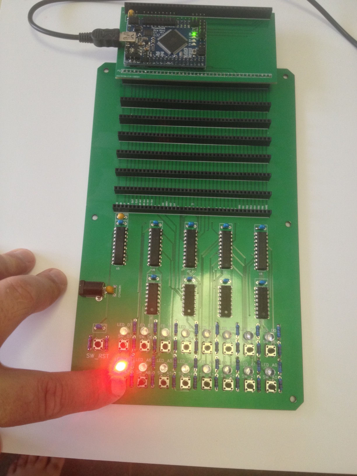
And D7:
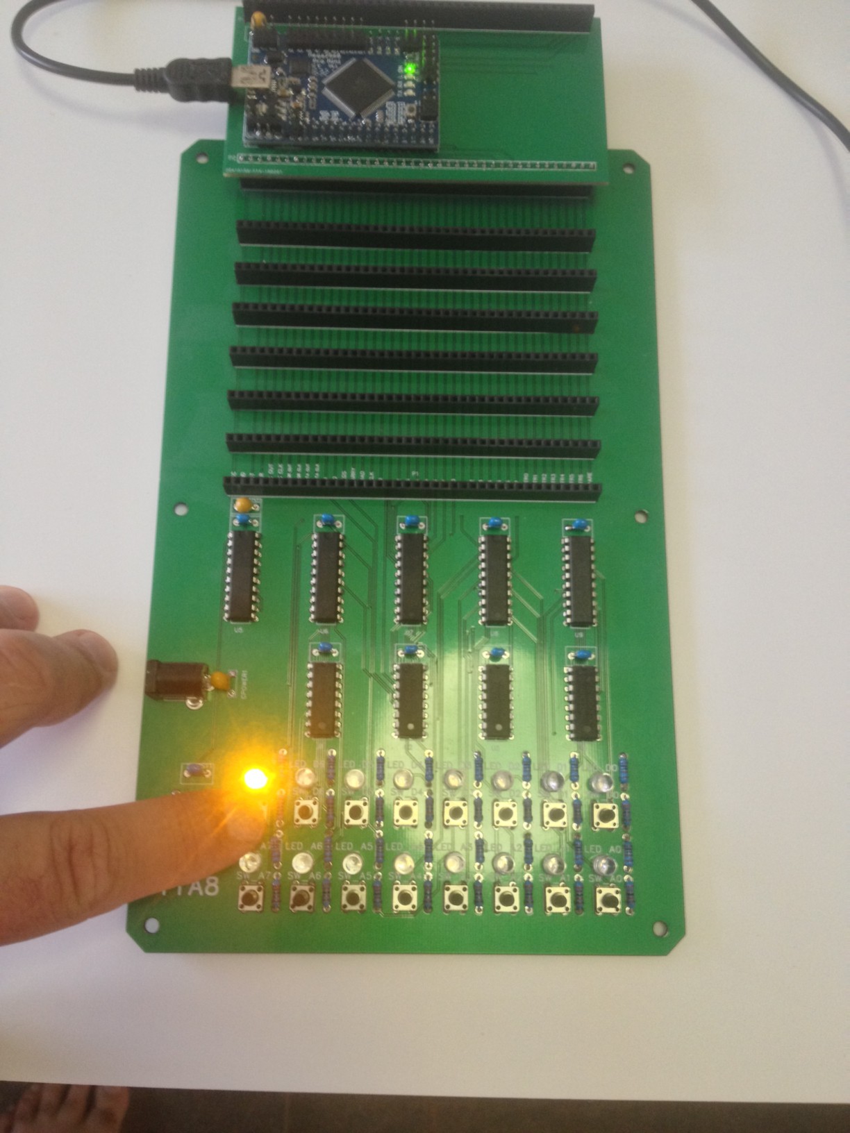
Trust me the rest work.
ALU Board
Next is the ALU Board. It works, no surprise as it tested out before.
ROM/RAM/StaticRAM Board
No it does not work. So far I have found two errors. The ROM page and RAM page are swapped, and the Static RAM (Addresses 192 to 247) are latched (wrong).
I forgot that the ROM/RAM pages are latched by a jump (i.e. JC or JMP).
For testing purposes I can fix these in software but still I cannot read the ROM or RAM data. I have to rework the code to make it easier to log the bus (i.e with a bus analyser).
Still no life out of the board. So the it is a chip select problem. Yes, U4 expects REGS high but I design REGS low.
Fix. I can't fix this in software so time for a new board.
Interrupt Board
This board generates SCLK which is 38400 Hz. It uses the WR signal from the Controller Board. There is always a WR (and a RD) every 8 clock cycles (no more and no less).
Interrupts Intr0 through to Intr6 are external while Intr7 is connected to a 2400 Hz clock (SCLK/16). The interrupt address is 0xFF (read only). Reading the interrupt address clears Intr7. Intr& is used to control the serial card (along with SCLK).
Anyway, my tests tell me the Interrupt/Timing Board is working.
Program Counter Board
This board is controlled by the Controller Board (which previously tested okay (at least by the logic analyzer)).
Other than the Serial Board, this is the last board to test.
New Paged Memory Board
Populated the new Paged Memory Board.
Plug in Mother Board - Fail.
Test the Paged Memory Card:
- Tested Paged RAM - check.
- Tested Static RAM - check.
- Tested Paged ROM:
- Page 0 - Corrupted.
- Pages 1+ - Okay.
Check FRAM in programmer:
- Check - Page 0 correupted.
- Reprogram FRAM
Recheck Paged Memory Card:
- Check - All good.
Plug in Mother Board - Fail.
Test the Paged Memory Card:
- Page 0 - Corrupted.
- Otherwise all good.
This means something is writing to the FRAM as the WR signal is exposed.
Could be code or hardware responsible.
Something to look at tomorrow, otherwise progress has been made.
---
I set Software Data Protection (SDP) mode on the AT29C256 FRAM.
At least I think I have? I will find out shortly.
Anyway should not have to reprogram the FRAM after each test.
Now to find out why, is it the Monitor code or a hardware problem?
AlanX
Discussions
Become a Hackaday.io Member
Create an account to leave a comment. Already have an account? Log In.