 radiona.org
ULX3S webpage
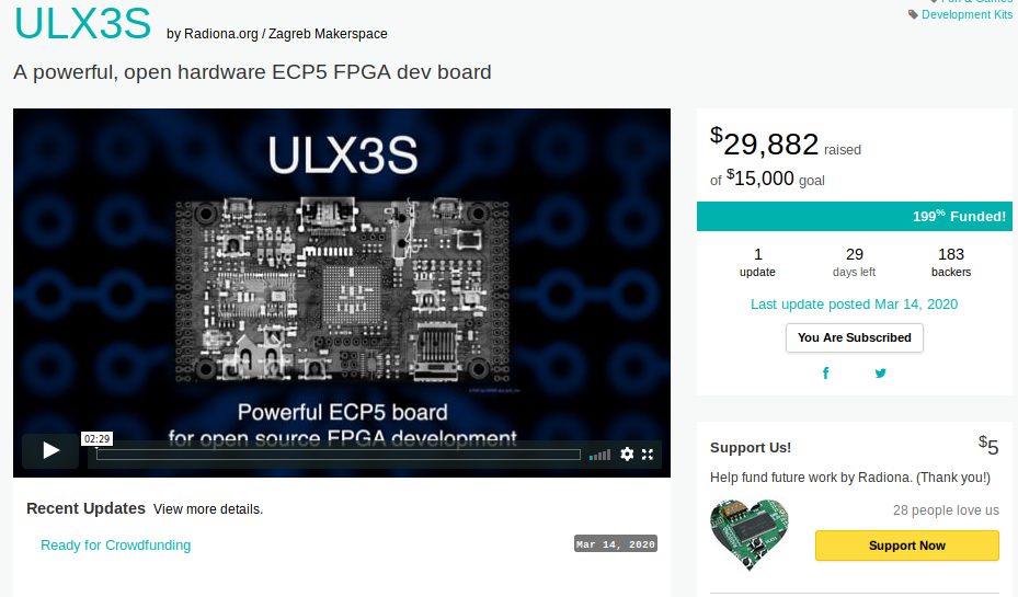
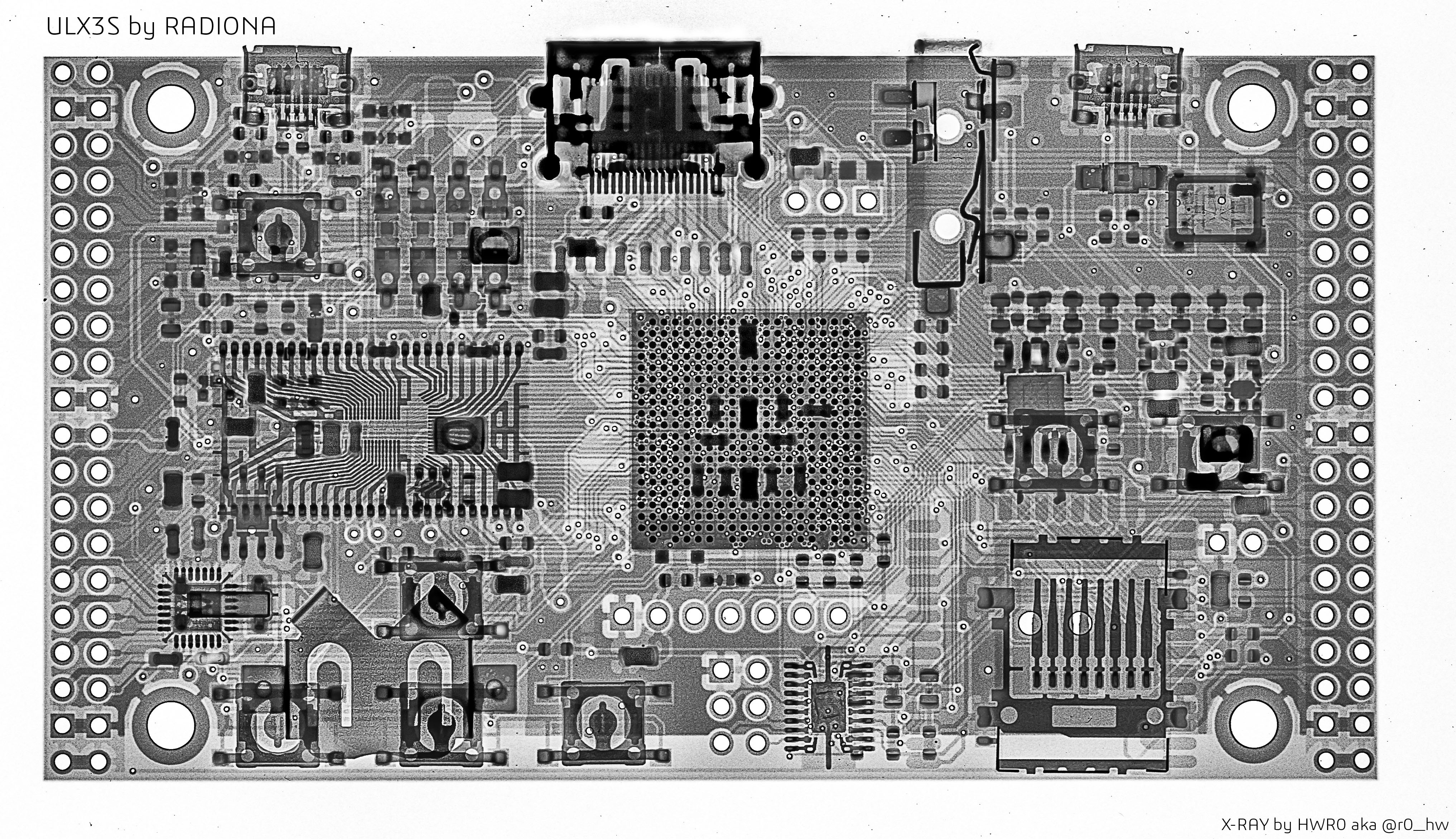
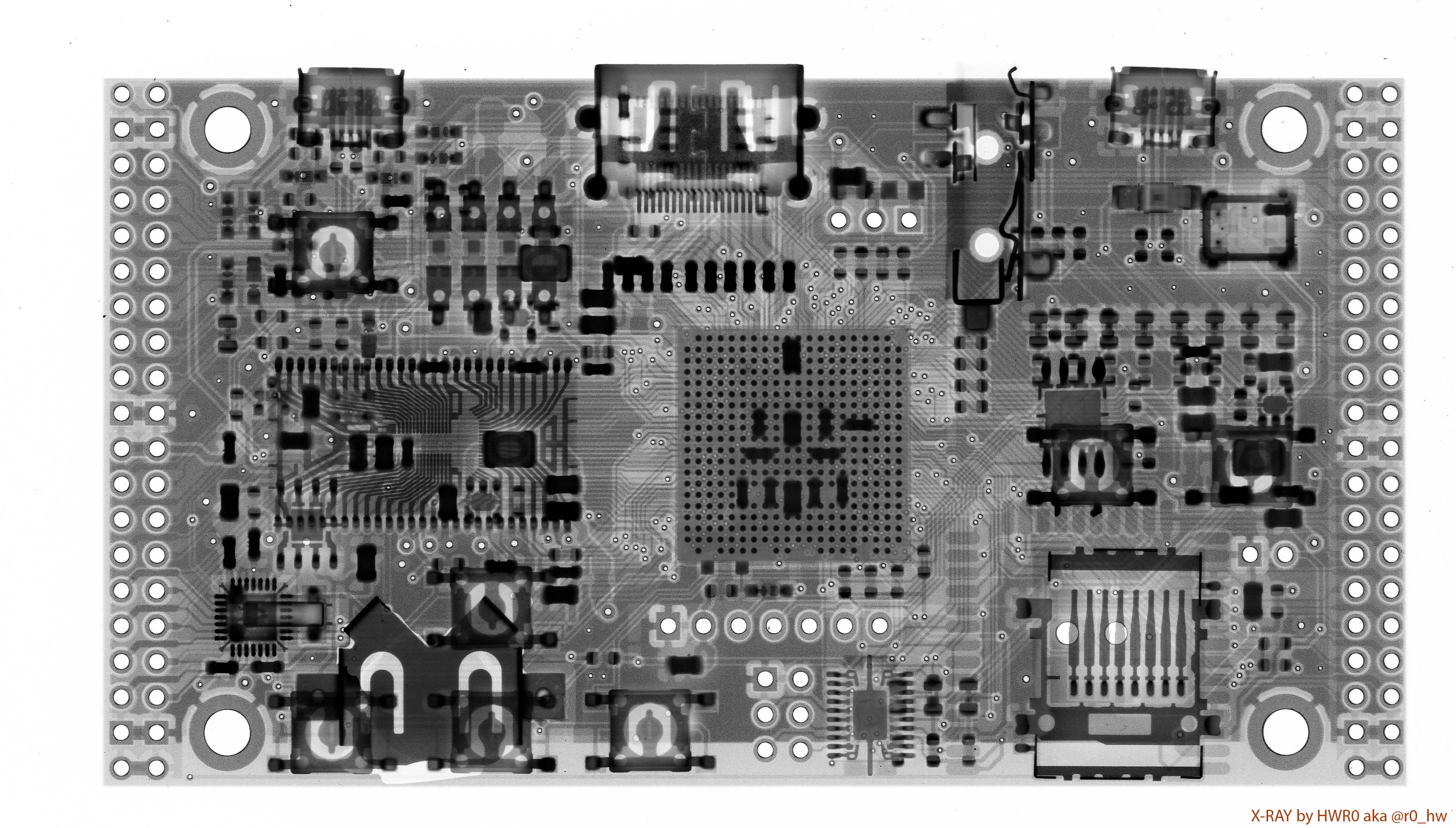
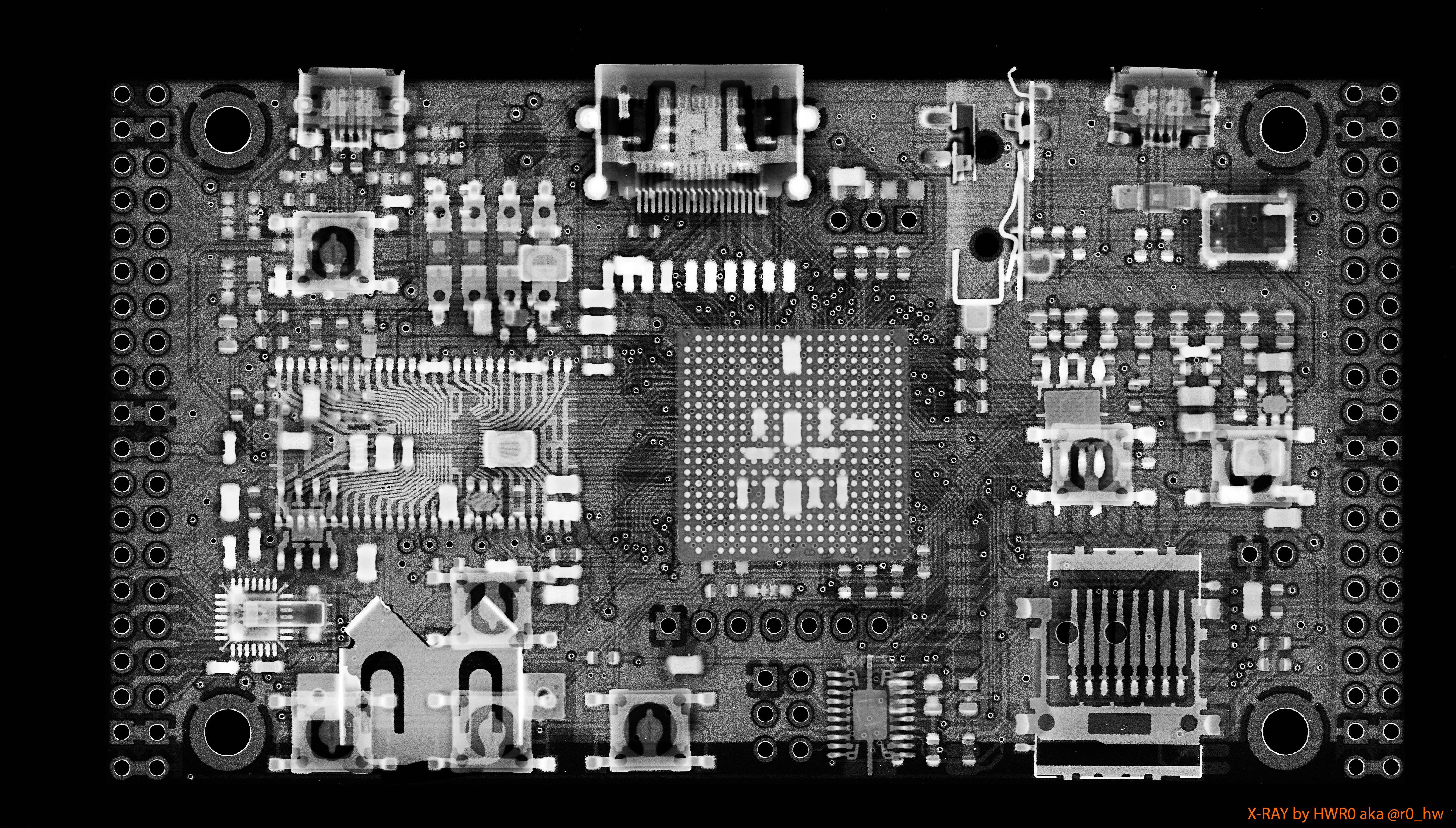
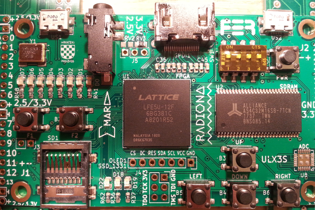
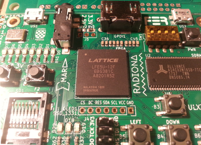
ULX3S uses powerful Lattice Semiconductor ECP5 series FPGA chip supported by the latest open-source toolchains. This makes the ULX3S one of the most powerful and desirable platforms for FPGA enthusiasts available today. ULX3S comes equipped with onboard WiFi, display, buttons, LEDs and storage. Flash it using the WiFi connection (over-the-air update), or with one of the bitstreams stored on SD card and browsed by onboard OLED display and buttons. Due to its battery-backed RTC, it can power down completely and wake up only on certain events making it useful for low power applications such as battery-powered remote sensor nodes. And if you’re not of the low-power type, onboard peripherals such as SDRAM, USB, Digital video out, onboard FM/ASK antenna, ADC and DAC can make it audio/video powerhouse for signal processing and synthesis, motor control or SDR cases. You can emulate arcade machines or retro computers like Minimig(Amiga) or modern systems like F32C (MIPS/RISCV). It has 56 GPIO pins, all routed as differential pairs and a PMOD compatible pinout, opening it to a wide range of expansion options. If you are just starting with FPGA, you can also use the ULX3S as powerful Arduino and program it using Arduino IDE in seconds.
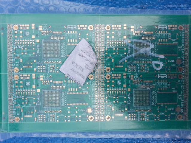
It has been actively developed since 2016 and is the result of collaboration between Radiona.org / Zagreb Makerspace and FER – Faculty of Electrical Engineering and Computing – University of Zagreb, Croatia.
1 ULX3S is beeing actively used in Digital Logic class at the University of Zagreb Faculty of Electrical Engineering and Computing, Croatia
Features
FPGA: Lattice ECP5 LFE5U-85F-6BG381C (85K LUT)
USB: FTDI FT231XS (300kbit JTAG and 3Mbit USB-serial)
GPIO: 56 pins (28 differential pairs), PMOD-friendly
RAM: 32MB SDRAM MT48LC16M16
Flash: 4MB Quad-SPI Flash IS25LP032D for FPGA config
Storage: Micro-SD slot
LEDs: 11 (8 blink-LEDs, 2 USB LEDs, 1 WiFi LED)
Buttons: 7 (4 direction, 2 fire, 1 power button)
Audio: 3.5 mm jack with 4 contacts (analog stereo + digital audio or composite video)
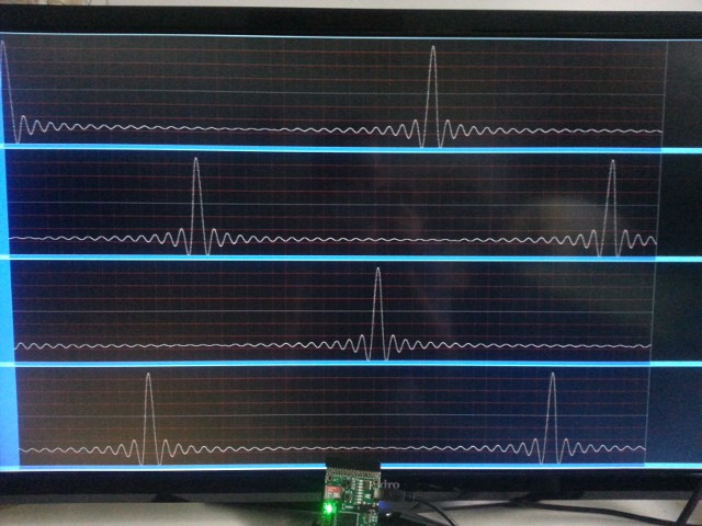
Video: GPDI connector with 3.3V-5V I2C bidirectional level shifter
Display: placeholder for 0.96" SPI COLOR OLED
WiFi+bluetooth: placeholder for ESP-32 (Standalone JTAG web interface over WiFi)
ADC: 8 channels, 12 bit, 1 MSa/s MAX11125
Power: 3 Switching voltage regulators: 1.1V, 2.5V, 3.3V
Clock: 25 MHz onboard, external differential clock input
Low power sleep: RTC clock wakeup, power button, 32768 Hz quartz and battery
GPDI is General Purpose Differential Interface, Electrically LVDS, mostly TMDS tolerant female receptacle more-or-less compatible with digital monitors/TVs
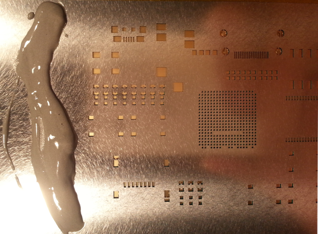 Applying solder paste.
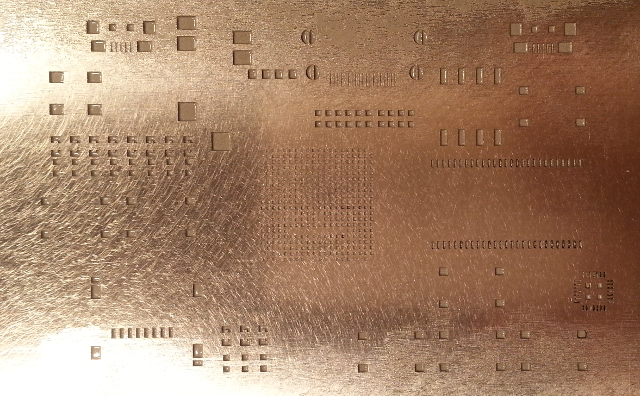 I looks fine!
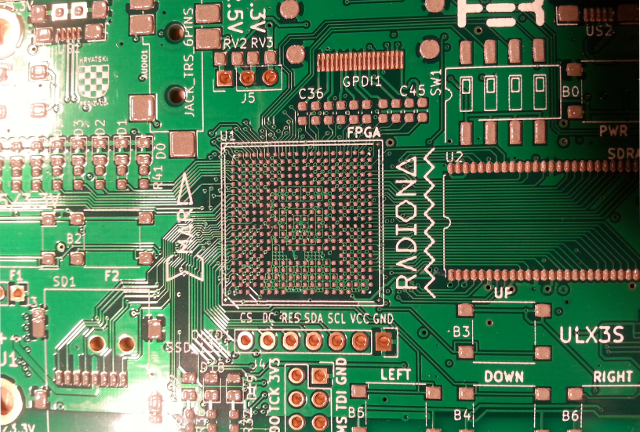
 Into the oven we go!!!
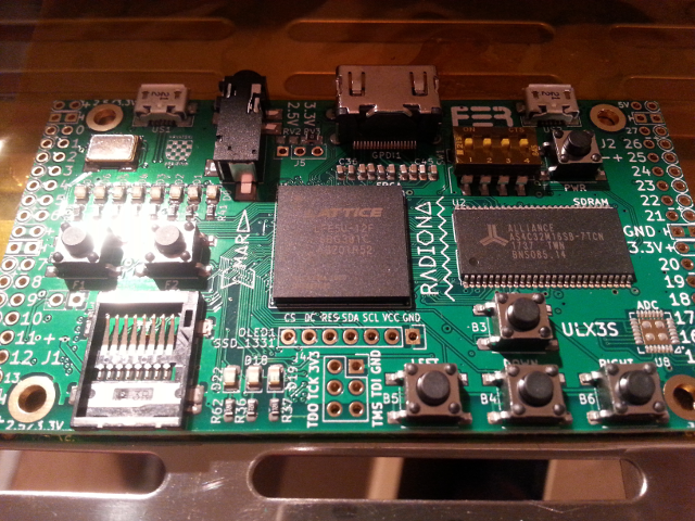
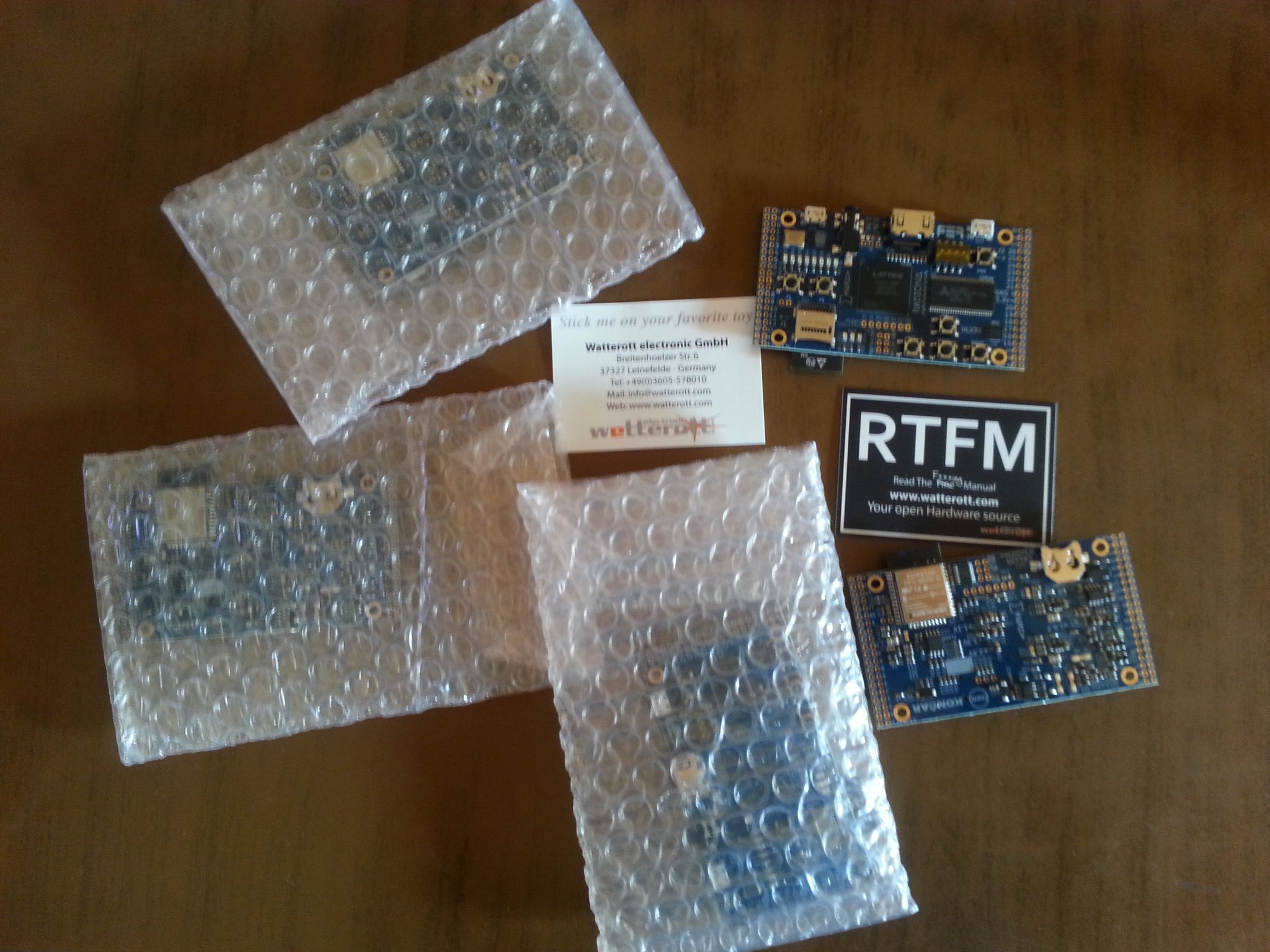
 Using donor board for power and FTDI - just to confirm all top parts are working...
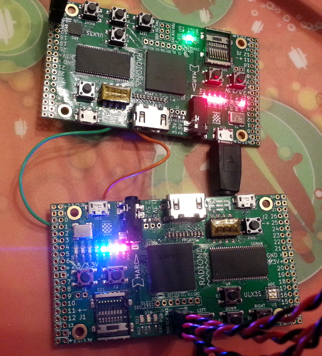


 Dan Julio
 pcadic
 Kris Winer
 Abraham
Curious where you get your PCBs made that can handle the tight annular rings you have around your vias (~4.3mils or .1095 mm)? Also how do you mount the BGAs?