 Al Williams
FPGAs are hardly new. But at first they were expensive and required expensive tools and design techniques. That hasn't been true for awhile and FPGAs are now cheap and starting to show up in lots of embedded systems -- even Arduino now has an FPGA/CPU combination. Are you ready for FPGAs? It seems like using an FPGA is like writing software, but it is actually quite different.
There are a few ways people tend to use FPGAs:
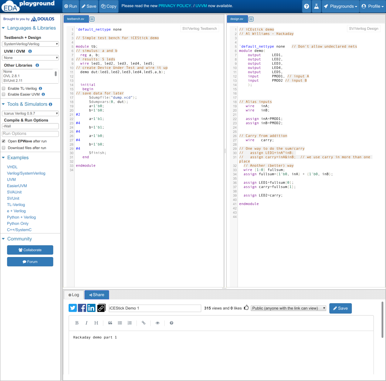
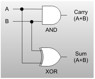
1) Replace logic gates like AND and OR gates, flip flops, etc.
2) Perform algorithms in hardware which can be very parallel either with or without a CPU
3) Provide custom I/O devices for a CPU
4) Build custom CPUs
(You can find more details about how people use FPGAs in the Project Log notes.)
This is part 1 of the bootcamp. You won't need anything special to follow along -- not yet, anyway. We'll use an online simulator that's available for free. You can also use any other Verilog simulator you like, if you'd rather use your own tools.
You should probably know a programming language like C or C++ before attempting this as it isn't a Verilog tutorial per se. Verilog looks a lot like C but it is actually quite different. While C is a language for specifying steps that a CPU takes, Verilog is a language for specifying what you want to happen. For example, if you specify a 7-segment decoder that takes 4 binary bits and lights LED segments in a display, the Verilog tools will realize what you want and build the equivalent hardware for it. That hardware doesn't execute step-by-step. It just "is."
Think about the light switches in your house. There's nothing saying "let me check the living room switch followed by the bedroom switch followed by the closet..." A CPU would work like that. But in your house -- and in an FPGA -- the switch is just connected to the light so when you flip the switch the light turns on. If you have one switch or 1,000 they all work the same way and take the same small amount of time to operate. Things don't "run" the way they do in a CPU, but just like you can think of all your light switches "running" in parallel , that's how FPGA hardware is.
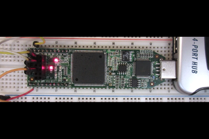
We will talk about the Lattice IceStick in this tutorial even though we won't use it until a later bootcamp. This is a $26 board that plugs into your USB port and even has open source tools available which we will use.
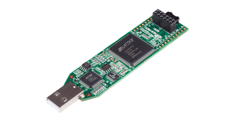
The IceStick has a modest FPGA onboard. From its manual, it has the following features:
- High-performance, low-power iCE40HX1K FPGA
- FTDI 2232H USB device allows iCE device programming and UART interface to a PC
- Vishay TFDU4101 IrDA transceiver
- Five user LEDs (one green and four red)
- 2 x 6 position Diligent Pmod compatible connector enables many other peripheral connections
- Discera 12Mhz MEMS oscillator
- Micron 32Mbit N25Q32 SPI flash
- 16 LVCMOS/LVTTL (3.3V) digital I/O connections on 0.1” through-hole connections
The FPGA isn’t huge (1,280 logic cells), but it is big enough to host a simple CPU. We aren’t going to start with a CPU, though. We’ll start with something much more simple.
OK, that's enough for this section. When you are ready, move on to the steps and get started on your FPGA adventure! You'll also find background articles in the project logs. You might want to browse them first and refer back to them as you work through the steps. The logs also have a glossary you can check for any unfamiliar terms.
This tutorial is part of a series:
| Bootcamp 0 | Covers basic digital logic concepts with simulations |
| Bootcamp 1 | Introduction to FPGA coding and simulation with combinatorial logic (this bootcamp) |
| Bootcamp 2 | More FPGA coding and simulation with flip flops (sequential logic) |
| Bootcamp 3 | Working with... |
 Luke Valenty
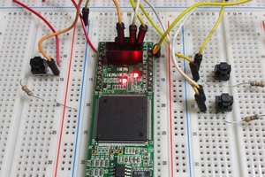
 Yann Guidon / YGDES