 Jurist
The first goal of this project was to build a prototype, to check following assumptions:
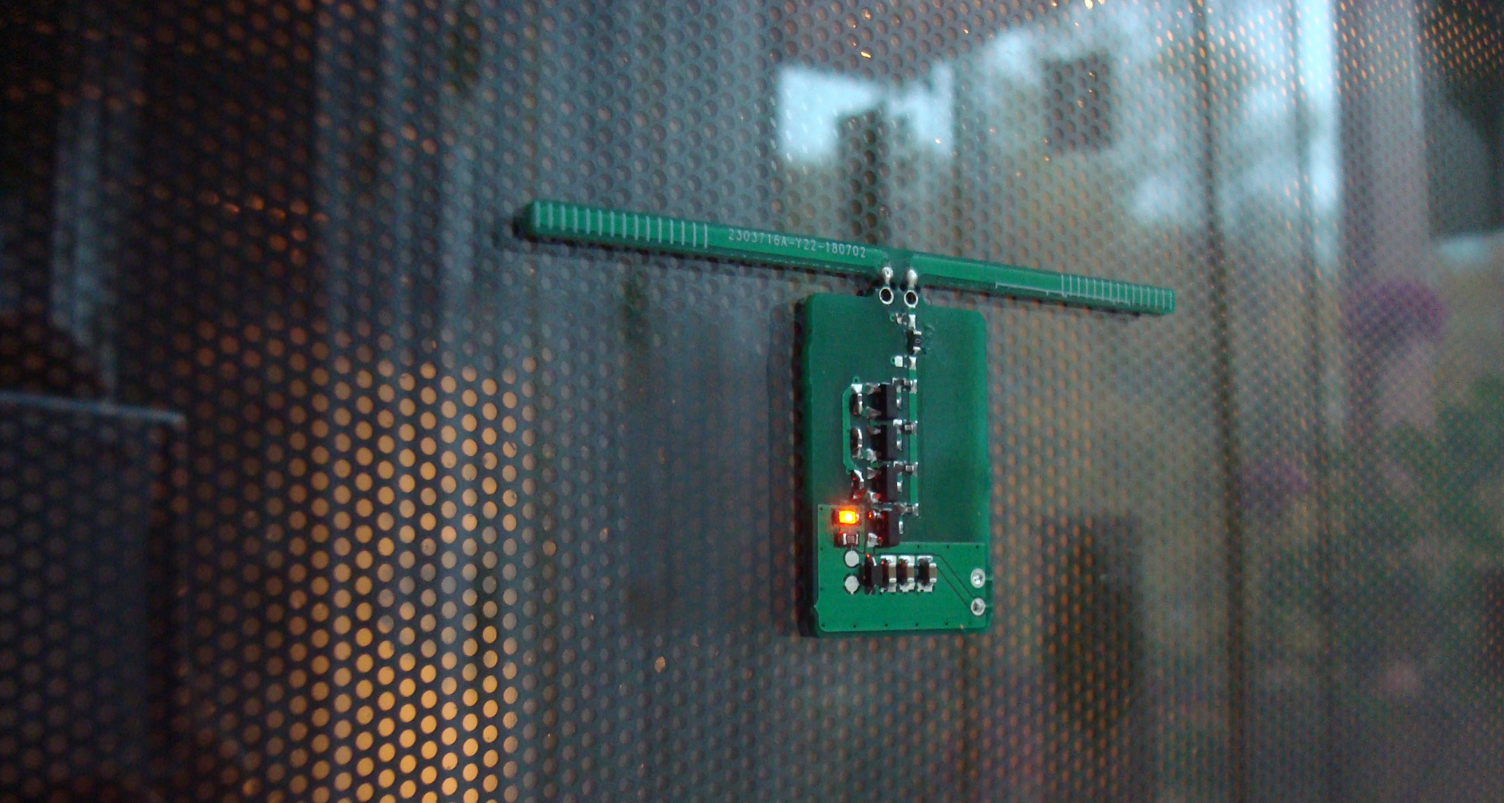
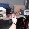
1) Some energy gets out of microwave oven in form of radiation (2.40GHz), although there is protective glass.
2) This energy is enough to collect it and power MCU
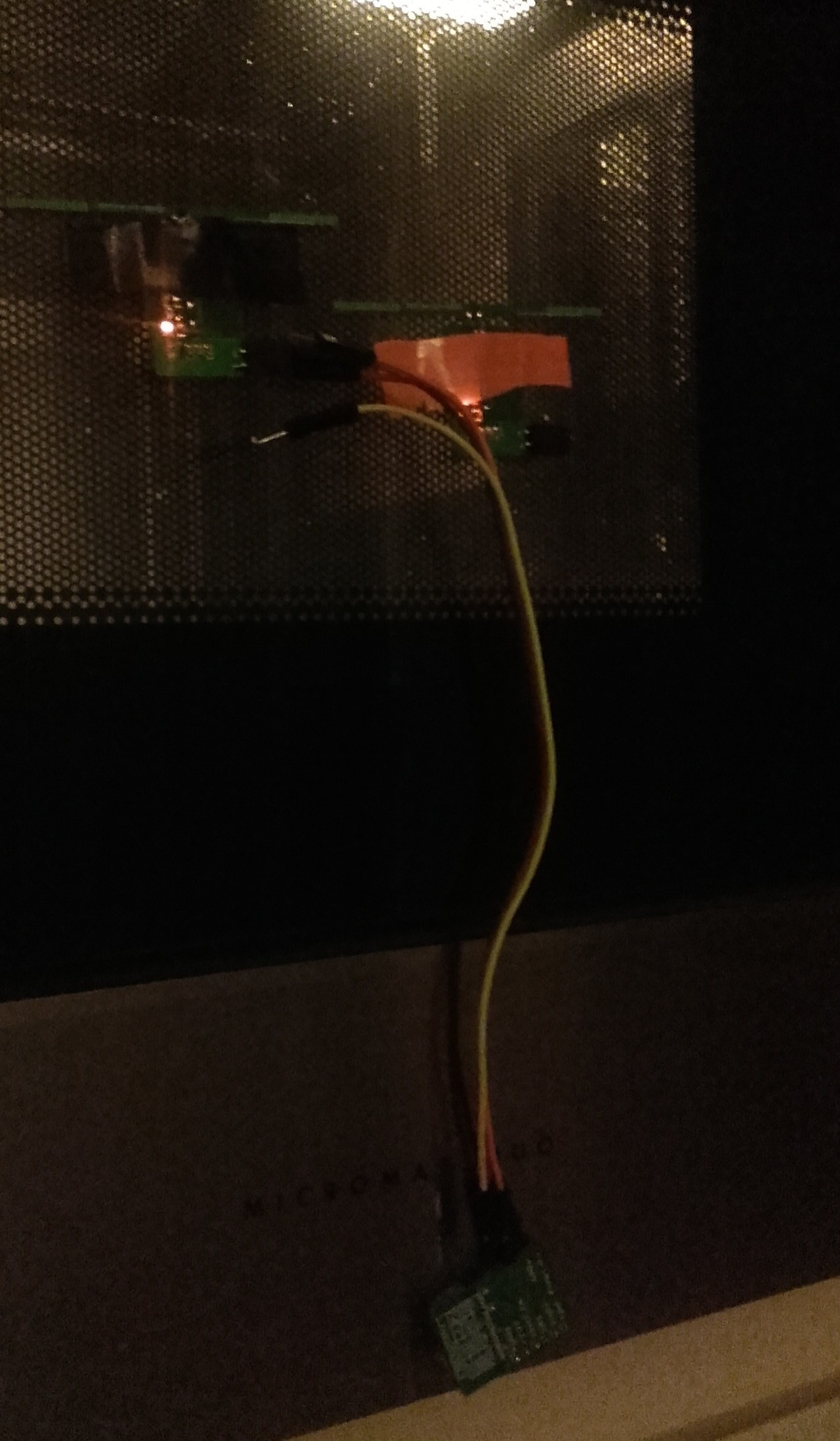
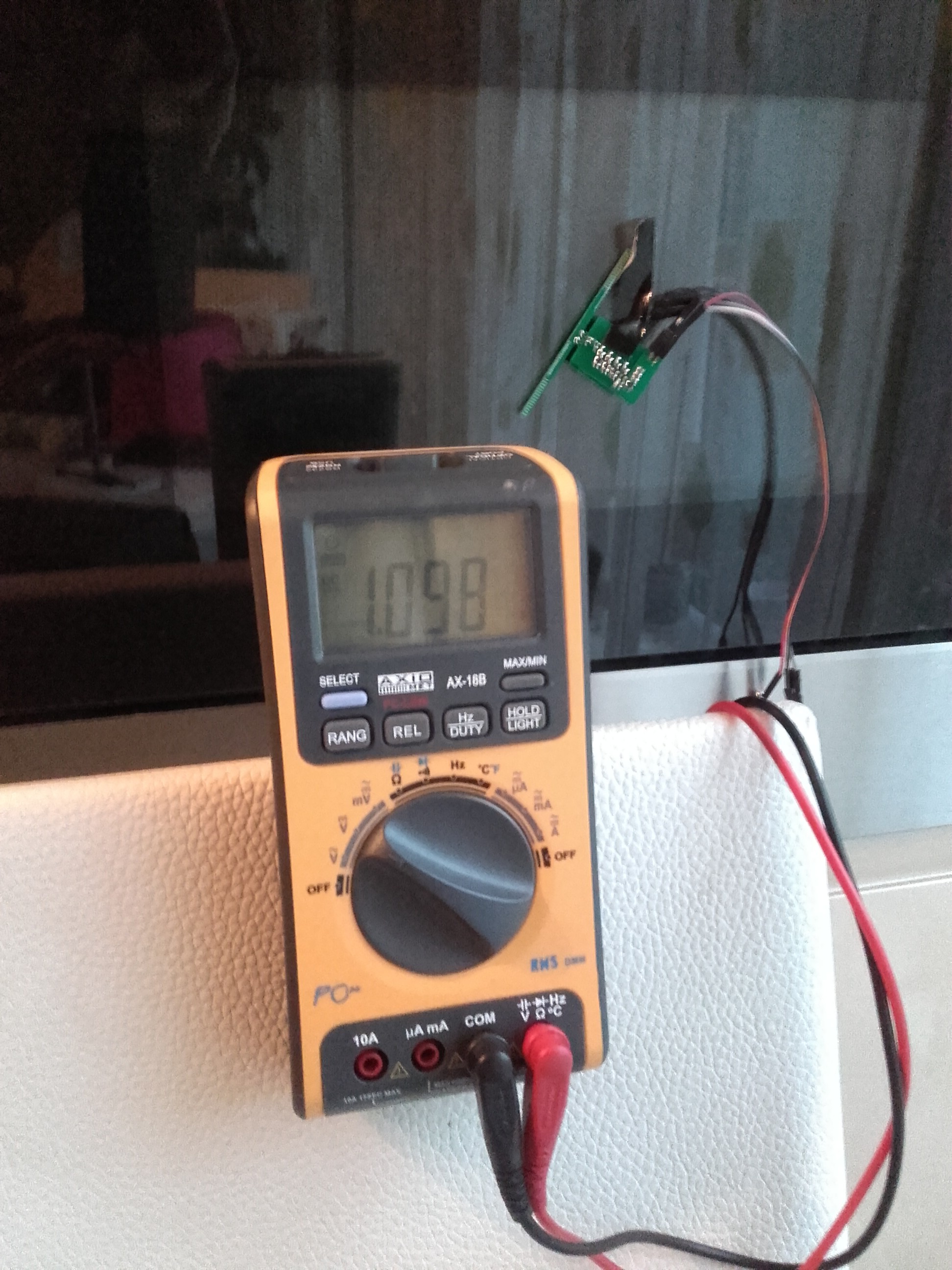
At this moment I can say, that p.1 is true, and energy is enough to lid a LED!
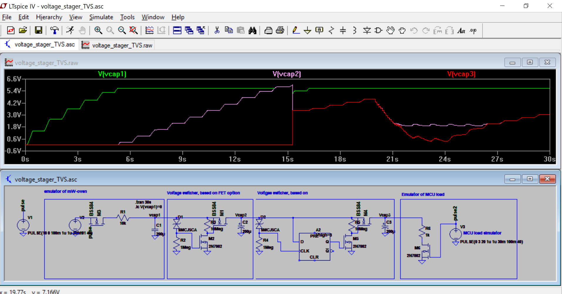
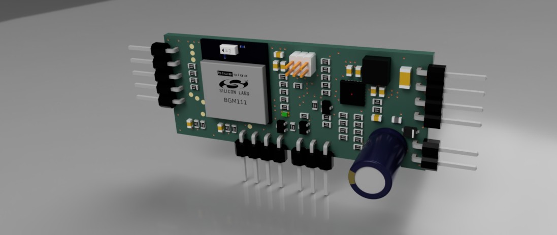
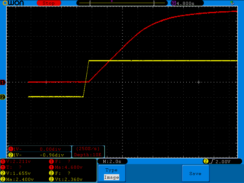
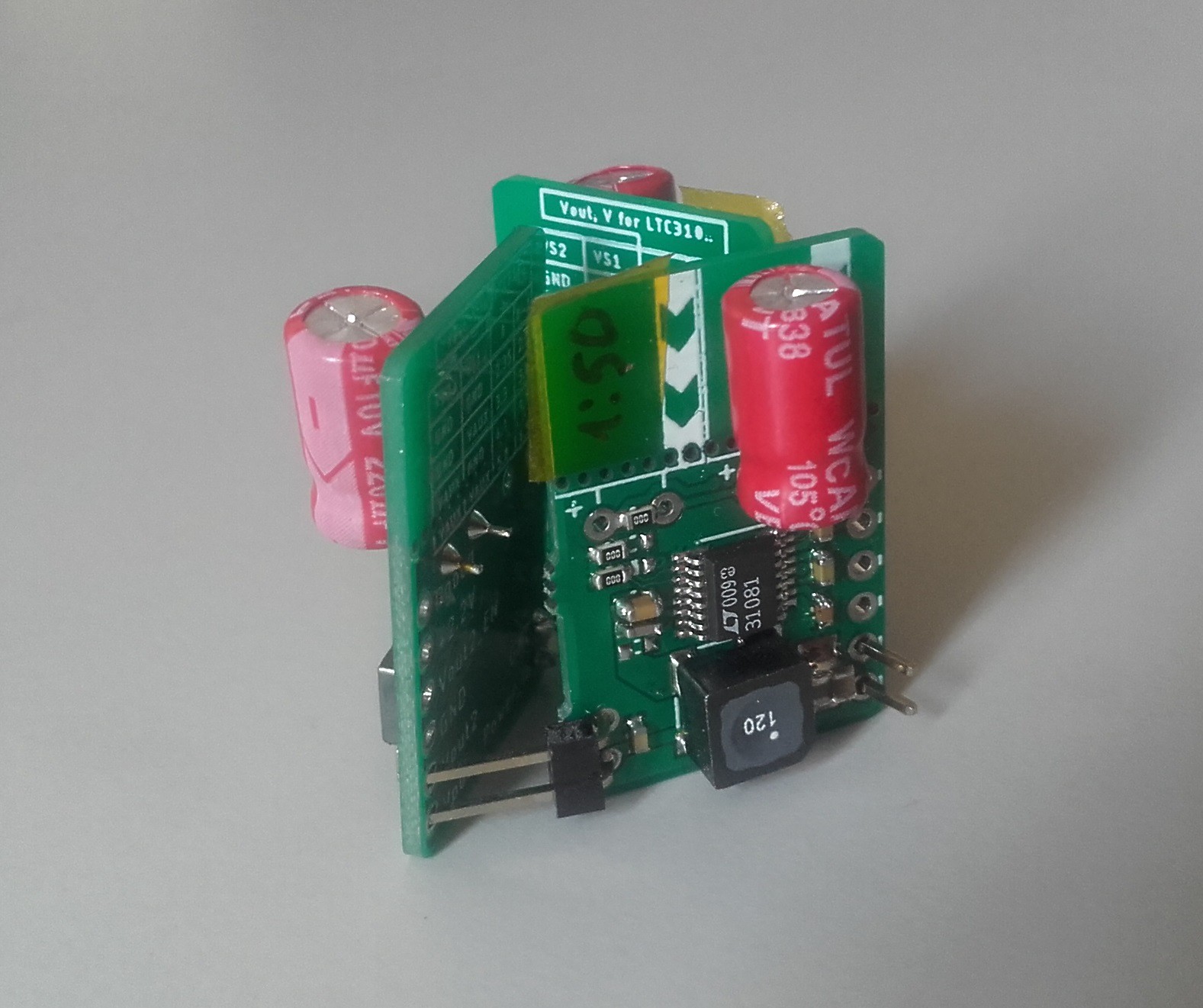
The other application of this PCB could be measurements of radiation beyond protective shielding of oven - just connect output of PCBA to ADC circuits (preferably buffered with opamp) of MCU, and you can see in real time the transformation of radiation into capacitor's charge.
p.2 - false: Some extra attempts have been taken, to make some energy-harvesting PCBAs , capable of transforming collected energy into something useful, to power MCU. However, at the moment, practice shows, that such circuit efficiency plus tiny quantities of collected energy are not enough for practical implementation.
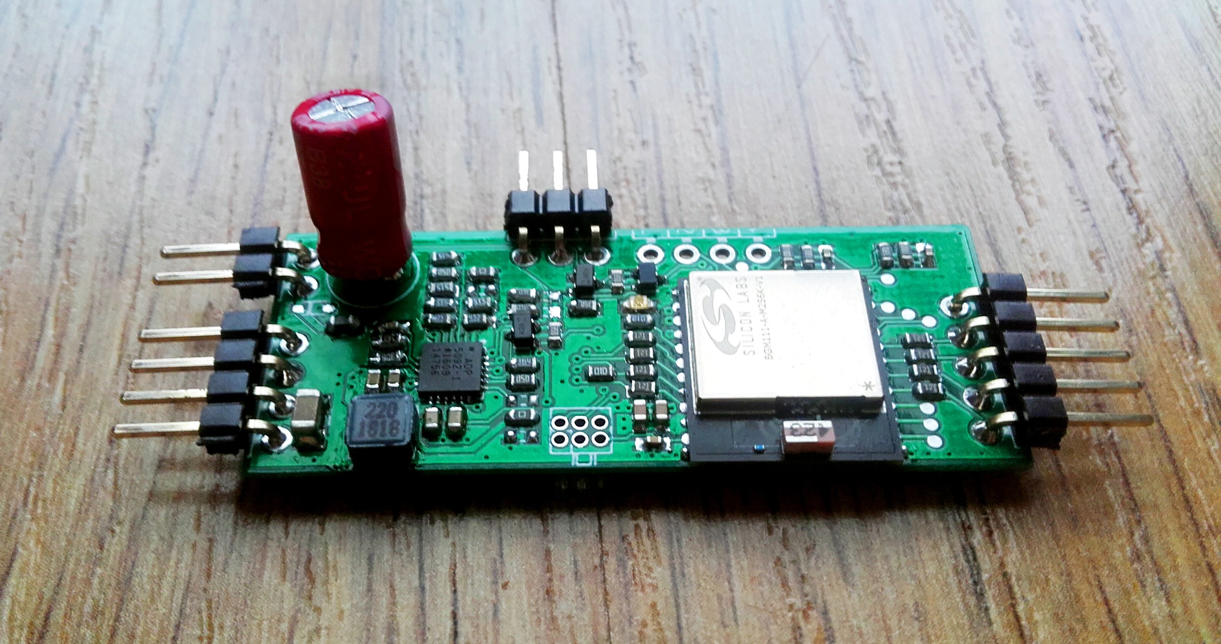

 and, actually, you can charge one of these boards from another, which charges from another one :D
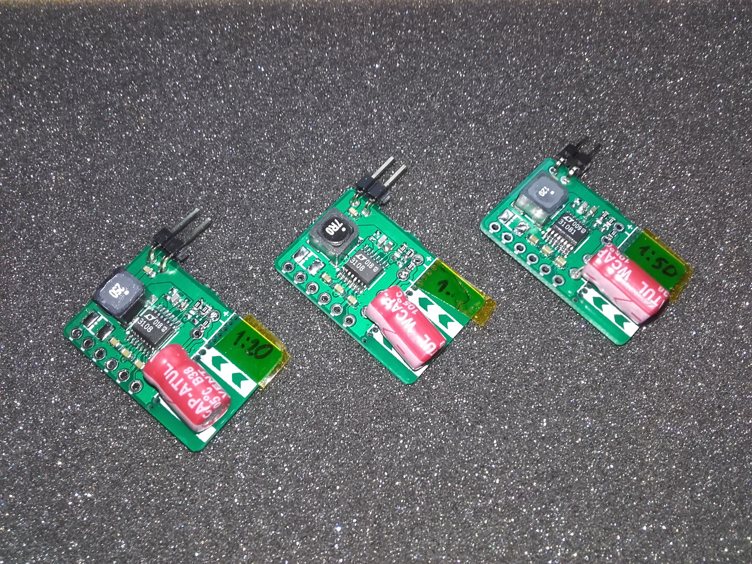


 Simon Merrett
 Guru-san
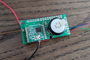
 strange.rand
>then it can be used to power MCU with BLE
Bluetooth Low Energy uses 2.4 GHz radio frequencies
- Would your BLE antenna pick up the leaked microwave energy and fry it?
- Would the leaked microwave at 2.4GHz interfere with your BLE?