 Peetselectronics
Settable logic gates
It use the cd4051 to set the input(A,B, C) the output(Q) to the desired value the jumpers on the switches(S1-S8).
On the upper left side, there are 3 inputs, A, B and C, you can connect *TTL signal directly to those pins. On the lower left side, you have the power pins, VCC and GND. Please do not reverse them, that will probably destroy your board.
*TTL signal explained: https://www.allaboutcircuits.com/textbook/digital/chpt-3/logic-signal-voltage-levels/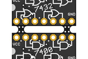
 JRodrigo
 DIY GUY Chris
 Pavel
Pavel
 LorneChrones (Nick)