Now it is much too hot in the attic to work on my RISC Relay CPU, thinking starts about a next project.
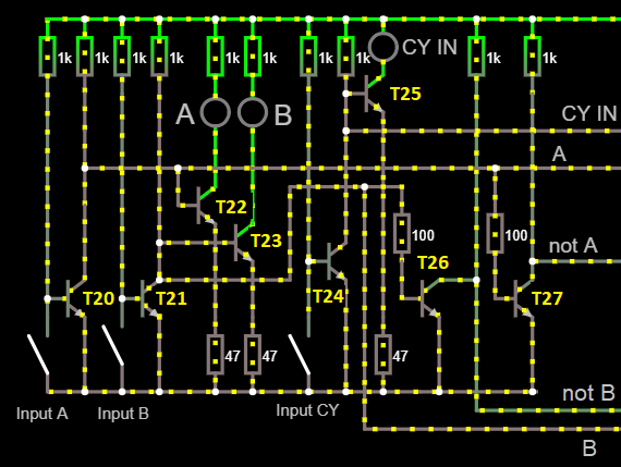
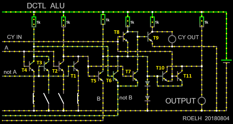
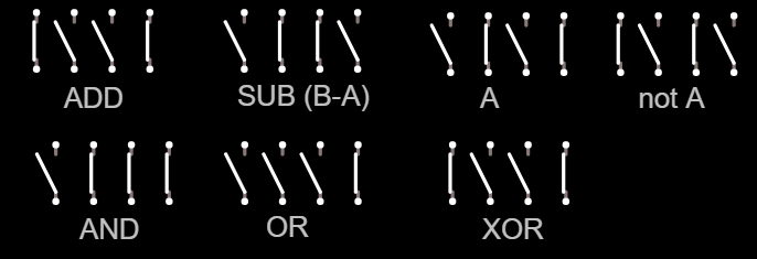
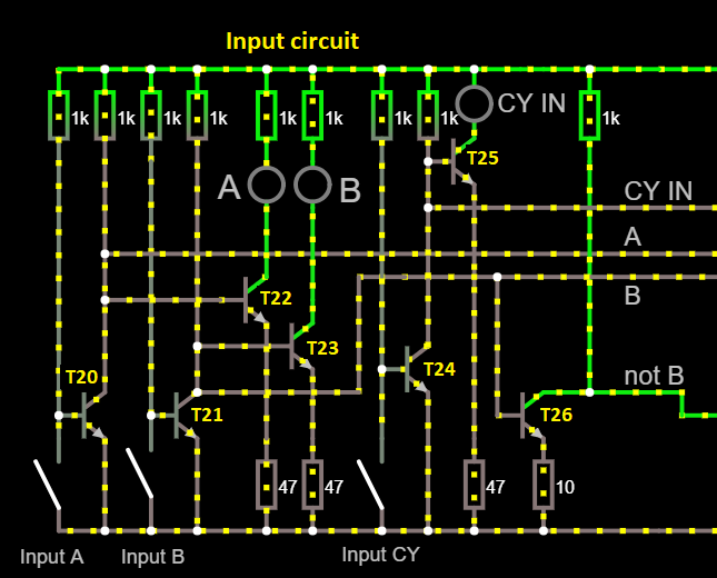
So I designed an ALU (wikipedia: ALU) in DCTL, that might be used in a next project. The ALU was simulated in the Falstad simulator, that has the nice property that you can actually see the current flowing during simulation.
The arithmetic and logical functions are all working correct. Optimizations for component values or speed have not been done yet.
For a discussion of DCTL, check Hackaday TTL-ers discuss DCTL and the Article of James Angell.
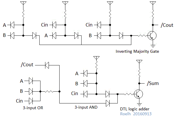
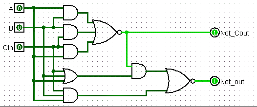
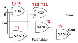
In a first log, I will show a full adder.
In the second log, this will be expanded to a ALU with ADD, Subtract and all 16 logic functions.
You can do the simulations yourself in the Falstad circuit simulator: In the File menu, select "Import from text" and paste the contents of one of the files in the files section.
My 4 bit TTL ALU on one square inch or One Square Inch TTL CPU might also interest you.

 Yann Guidon / YGDES
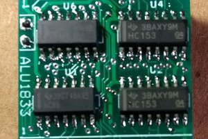
 will.stevens
 Tim
Tim