-
Subtraction
08/16/2018 at 17:26 • 0 commentsThe circuit description, as given in the first log entry, does not provide subtraction.
This was added by simply putting four exclusive-or-gates in the lines for the A inputs.
The function input F0 is now used to control these exor gates, and is no longer connected to the multiplexers. These inputs of the multiplexer are connected to logic zero. They were used for negating the B input, but negating an input can now be done with the new exor gates.
-
The fast carry circuit
08/15/2018 at 20:07 • 0 comments![]()
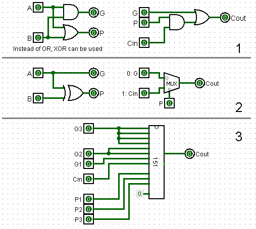
The first diagram is the classic carry circuit. The left side uses the two inputs A and B to generate P (propagate) and G (generate) signals. The right side shows how P and G, together with the carry input, produce the carry output signal.
In the first diagram, when G=1, the P output is actually a don't care. But for our solution, P must exactly represent if the input carry must be propagated to the output. We can do that by generating P with an exclusive-or (2nd diagram). Now, when P is active, we activate a switch (the mux) to connect the output carry to the input.
What to do when P is not active ? If P is not active, there are only two input situations:
1) A=0 and B=0 2) A=1 and B=1.
Only in the 2nd case, a carry must be produced. So, we can simply connect the second multiplexer input to A (or to B, since A and B are the same when P=0).
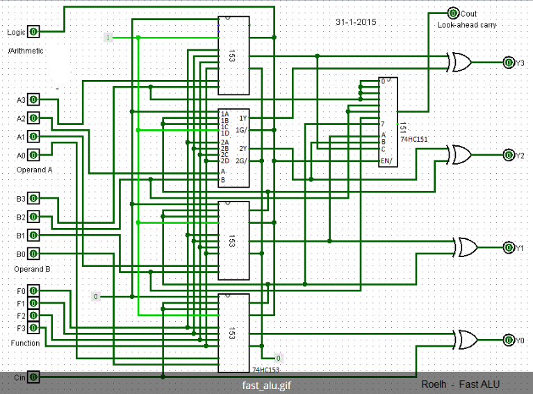
In the third diagram, the multiplexers of three adjacent bits are combined into a single 74HC151 8-input multiplexer. So for 3 adjacent bits, the Cin has to pass only a single IC before arriving at Cout. Note that the 151 has an enable input, that can be used to disable the carry for the logic functions of the ALU.
And as an extra bonus, since the P signals are "A exor B", they are exactly the same as the signal that is used to produce the sum (the RED wire in the diagram on the previous log). So, the generation of both P and G actually comes totally for free !
[ edit oct 2023: re-inserted the picture that disappeared ]
-
The Multiplexer is the heart of the ALU
08/15/2018 at 19:44 • 0 commentsI did spend a lot of time finding optimal ALU solutions.
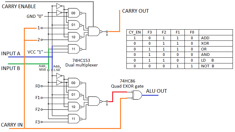
The best I could find (for TTL) was this:
![]()
[ Please note that the function table shown here is a little different from that of the Square Inch ALU ]
The key to the schematic is, that a single multiplexer (the lower one), can generate every possible logic function of two variables. (Only the the most useful ones are in the table).
For logic functions, all orange carry wires should be "0" (The grey CARRY ENABLE signal must be low to accomplish this for the carry output, the connection of the grey wire to the multiplexer is not very obvious, the multiplexer symbol that I used in the drawing did not have an ENABLE input). The output of the ALU is equal to the logic output (on the red wire).
For addition, the upper multiplexer part will generate the "majority" function of the 3 inputs, giving the new carry at its output. The incoming carry is exor'ed to the logic output (logic function should be set to XOR for addition).
The ALU can also pass one of the input signals unmodified, so it can be used for a LOAD instruction to get immediate or memory data into one of the registers. For the control section, the LOAD is just another arithmetic instruction, this simplifies the control section of your CPU.
With the addition of a 74HC151, it is possible to do a fast-carry that calculates a carry for three levels at once.
![]()
The above schematic can easily be adapted to relay or other technologies.
For a relay based ALU, see the file "relay CPU technology V1.7" in the files section of https://hackaday.io/project/11012-risc-relay-cpu, that is based on the same idea. The logic function is performed in diode-resistor logic, combined with relay logic.
A transistor version can be found HERE.
(A previous version of this log was a comment made to AMBAP in 2016)
[ edit oct 2023: re-inserted the picture that disappeared ]