Skoll – Xilinx™ Kintex™-7 USB Ready To Go FPGA Module
Ok, we have a module and tools ready now, let’s try to run a simulation on the module and see if it works as expected. In order to simulate the module, we need to give some input to the module, how we do that? The answer is, we need to create a test bench! The test bench will generate the necessary inputs for the module under analysis (Here “myModule”). A test bench is nothing but another Verilog module which generates some signals and feeds it to the module under test. During simulation, the test bench should be a “top module” (top-level module) with no I/O ports. But when it comes to implementation on real FPGA, the “top module” can have I/O ports and test benches won’t be the top modules there (we will talk about this in detail later). So here goes the test bench code.
module myModule_tb();     wire out;    reg clock;         always begin
	#1 clock =!clock;    end         initial begin
	//Initialize clock
	clock = 0;     	//End simulation
	#10
	$finish;    end         myModule notGate(clock, out);

endmodule
Let me break this down for you.
The test bench is just another module, with no I/O ports as I mentioned earlier. I have created a wire named “out” and a reg named “clock”. We will create a clock on reg “clock” by periodically inverting it and feed it to the input (port A) of myModule. The wire “out” is connected to the output port (port B) of myModule. The result should appear on the wire “out” in the simulation.
The “always” block is something worth special mention here. As the name implies, “always” block will keep on executing as long as the simulation is running. In real-world designs, “always” blocks are a little more complicated with sensitivity lists etc…. But for this simulation, the simplest form of “always” should suffice. I’ll discuss this in details in later chapters.
In the “always” block the reg “clock” is inverted after every one-time unit delay. The symbol # is a way to specify a delay in Verilog. So the always block executes always, and inside the block, “clock” is inverted continuously so that the waveform on clock looks like a square wave. Remember that # symbol is not a synthesizable element. We have to find some other way if delay needed in our design when we synthesize the code. But it works just fine for simulation.
The next block is an initial block. As its name suggests, this block will be executed only once at time t = 0. So anything that we need to initialize should go here. Initial block also is usually used only in test benches. Initial blocks are rarely used in synthesizable code, instead, reset logic is created if initialization is required. We initialize the reg “clock” to zero. This is very important. If we don’t initialize a register, its value is considered as unknown and no matter how many times an unknown is inverted, the result will always be unknown. That is, if we leave “clock” uninitialized, “clock” won’t be generated. The last part of the initial block is the $finish directive. The $finish directive is placed after a 10-time unit delay, this means after simulating the design for 10-time units, stimulator will stop running. All functions start with the $ symbol is called tasks. Tasks are merely commands to the simulator, they don’t alter the circuit behavior.
Last but not the least, the module instantiation. The statement “myModule notGate(clock, out)” creates an instance of the module “myModule” with name “notGate”. You can create as many instances as you want from a module. One really important thing here is the wiring. If you look at the code, you can see the reg “clock” placed as the first parameter and the wire “out” is placed as the second parameter. This literally means that the reg “clock” is connected to port A of the module instance and wire “out” is connected to port B of the module instance.
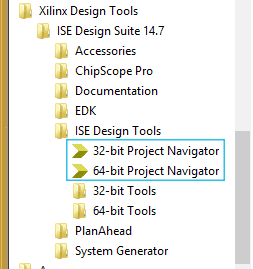
Now it is time to run the simulation. Follow the steps below to run the simulation in Xilinx ISE Webpack (Images are based on Xilinx ISE Webpack 14.7).
- Runs ISE Project navigator from the Windows program menu. Select 32 Bit or 64 Bit version of ISE depending on your Operating System.
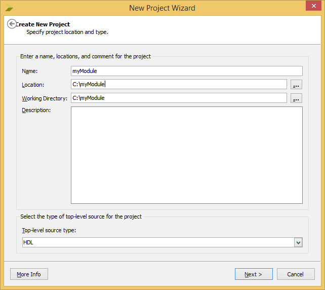
- From the File menu, select “New Project”
- Name your project and select a directory to save the project and click next (refer to the picture below).
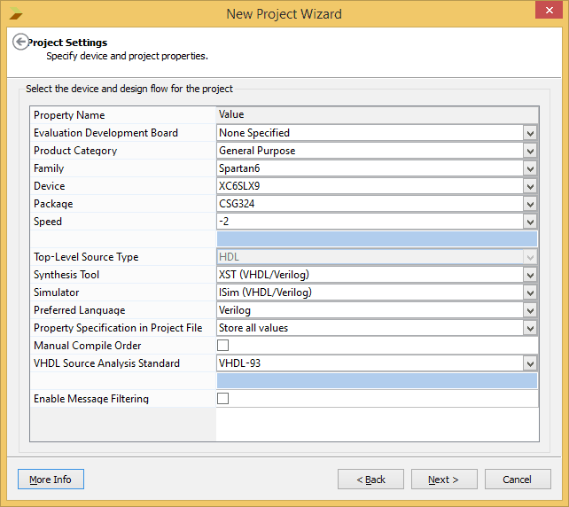
- Change the project settings as required. You can select the FPGA family and device based on the board you use. For Mimas V2 Spartan 6 FPGA Development Board it should be set as in the image below. For Elbert V2 Spartan 3A FPGA Development Board, the device family will be “Spartan 3A and Spartan 3AN”, Device will be “XC3S50A”, Package will be TQ144 and Speed will be -4. Once the information is filled in, click next and then finish.
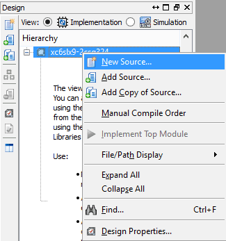
- We have created an empty project in Xilinx ISE Webpack. Now right click on the project and select “New source” from the pop-up menu.
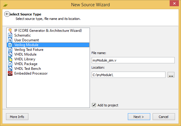
- Select “Verilog Module” as the source type and type in the file name as shown in the image below.
- Replace the autogenerated module template (or the contents of the whole file) with the code below.
module myModule_tb();     wire out;    reg clock;         always begin
		#1 clock =!clock;    end         initial begin
		//Initialize clock
		clock = 0;     		//End simulation
		#10
		$finish;    end         myModule notGate(clock, out);
endmodule

module myModule(A, B);    input wire A;    output wire B;    assign B = !A;
endmodule
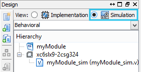
- Now make sure that we are in the simulation mode by selecting “Simulation” in design view
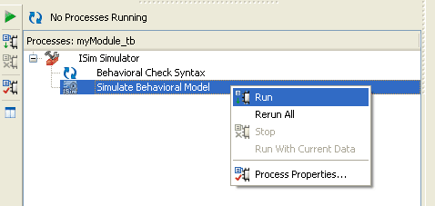
- Start simulation by right clicking on “Sim” process in the process view and selecting “Run” (The Verilog file myModule_sim.v must be selected in the Design View for this option to be visible).
- Now the ISim simulator will start and you will be presented with a simulation waveform like the one below (Sometimes you may have to zoom in/out a little bit to see the waveform correctly).
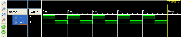
Inspect the waveform and make sure that our Verilog module is working as expected. As you can see in the image above, the output is the inverted form of the input clock. This is exactly what we expect from a NOT gate. In part 4 of this tutorial, we will implement this module on a real hardware.
Download complete Xilinx ISE simulation project for mimas V2
Download complete Xilinx ISE simulation project for Elbert V2
Original post: https://numato.com/kb/learning-fpga-verilog-beginners-guide-part-3-simulation/