 Mark Omo
Here is a description of how the analog fronted on our oscilloscope works.
The very first thing that happens is our signal goes into a 1M ohm terminator that also divides down our signal by 10X, allowing us to measure signals outside of the rails (up to around 30V Pk-Pk or ±15V). The very next thing that happens is the signal is passed through a pair of diodes connected to the rails that clamps the voltage to the rails preventing damage.
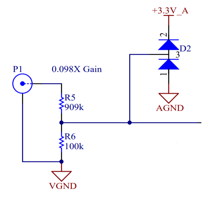
Notice how the divider goes to VGND, this is a signal that is halfway in between AGND and +3.3V_A so the incoming AC signal is centered around 1.65V. The other thing to note is that the 909k Ohm resistor is in-between the signal and the diodes so in the event of an over-voltage the current through the diode is limited to a small value (for example in the event of a 100V signal the current would be limited to about 100μA, of course there is not sufficient isolation to make 100V safe...).
The next step in the signal chain is the variable gain stage, that provides 10X gain, 5X gain, and 1X gain to allow for 3 total system gains, 1X, 0.5X and 0.1X gain. There are two main components of this subsystem, a TLV3541 op-amp and a ADG633 triple SPDT Analog Switch. Our op-amp was chosen to provide a power bandwidth (slew rate limited bandwidth) at around the response of our system. We had the same driving concern for the analog switch.
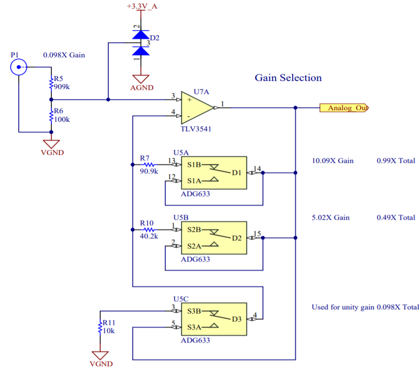
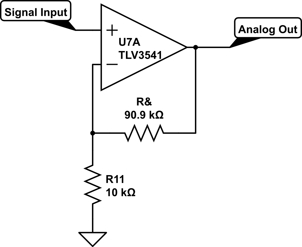
We can follow the signal path for the Gain Selection system now, to select 10X gain (for a total gain of 1X) we set D1 to connect to S1B and connect D2 to S2A (to remove the influence of R10) and connect D3 to S3B. Our circuit now looks like the one below:
We can change the contacts to select 5X in the same way, and disconnect R7, R10, and R11, just connecting the inverting input to the output to select unity gain.
When using analog switches like the ADG633 there is a trap for young players, the resistance of the switch is not negligible and varies with voltage sometimes significantly, here is a snapshot from the datasheet:
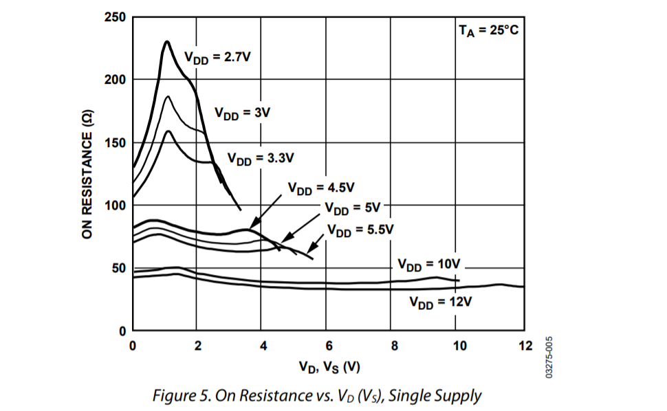
You can see that the on voltage can be as high as 240 Ohms and can vary significantly with applied voltage, luckily in our application the screen we were using needed 12V so we could supply 12V to the mux to get a much lower on resistance and a much flatter response over our region of interest(0V-3.3V). The average on resistance at 12V of 45 Ohms is less than the tolerance of our resistor part (we used 1% resistors across the board).
The next major section of the system was the ADCs, we used the PIC32MZ1024EFH064. The ADC module on the PIC32MZ is a 12-Bit Successive Approximation ADC. One of the advantages to a SAR ADC is that every extra bit of resolution takes a constant time, i.e. converting with 12-Bit accuracy takes twice as long as converting with 6-Bit accuracy so you can trade off speed and accuracy of the ADC.
The ADC module runs at a slower clock than the main core (in our case it runs at 50Mhz), every 20 nanosecond (1 50 Millionth of a second) period is called Tad (Time A to D) and the time everything in the ADC module takes is measured in Tads.
An ADC conversion starts with the sample and hold sequence, essentially there is a switch between the Microcontroller pin and the sample and hold capacitor and it takes some amount of time to fill that capacitor (it depends on the source impedance). We are driving it directly from an Op-Amp so we can assume a very low source impedance, so we can use the shortest sample and hold time 3 Tad or 20ns.
The next step is using the stored voltage on the capacitor to calculate the voltage and that time depends on the bit-depth selected:
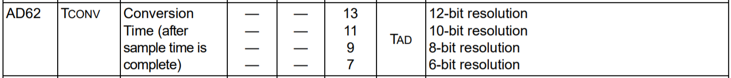
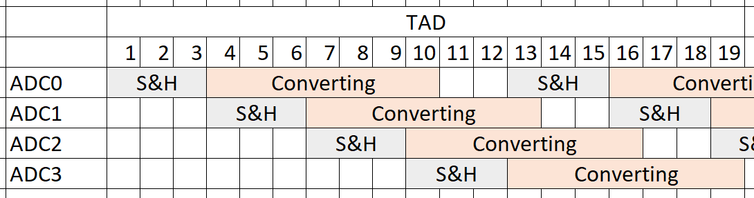
We chose to use 6-Bit mode to give us the fastest conversion time (and becouse our screen is only 64 pixels tall or 6 bits tall). However this gives a total conversion time of 3 Tad + 7 Tad = 10 Tad or 200ns, only 5 Mega Samples Per Second. In order to get an even faster sample rate, up to our 20Msps target, we need to use a technique called interleaving.
Interleaving works by using several ADCs in parallel to sample at the same time. This allows us to get a much faster sample rate, the picture below shows how the system works.
In order to cope with the 120 Megabits per second of data coming out form the ADC module we take advantage of the Direct Memory Access (DMA) peripheral available on the PIC32MZ, it gives us the ability to write the data coming from the ADC directly into the memory of the Microcontroller without having to involve the processor at all.
Discussions
Become a Hackaday.io Member
Create an account to leave a comment. Already have an account? Log In.
I am surprised that you don't have an anti-aliasing filter at the ADC input?
Are you sure? yes | no
This was something we overlooked in the design as it was rushed to release, however the 900k input resistor forms a first order low pass filter with the parasitic capacitance of the op-amp and the diodes that gives our system it's 1 Mhz bandwidth. Future improvements might include (space permitting) a compensation circuit on the frontend to allow for more than 10 Mhz of bandwidth, and a 4th order Low pass Anti-Aliasing filter after the op-amp. Coupled with software anti aliasing we should be able to tune it for 3.5+ Mhz of bandwidth.
Are you sure? yes | no
Great explanation, thnx!
Are you sure? yes | no