 greg davill
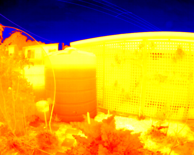
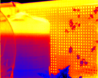
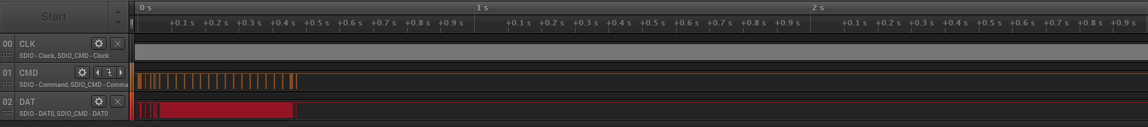
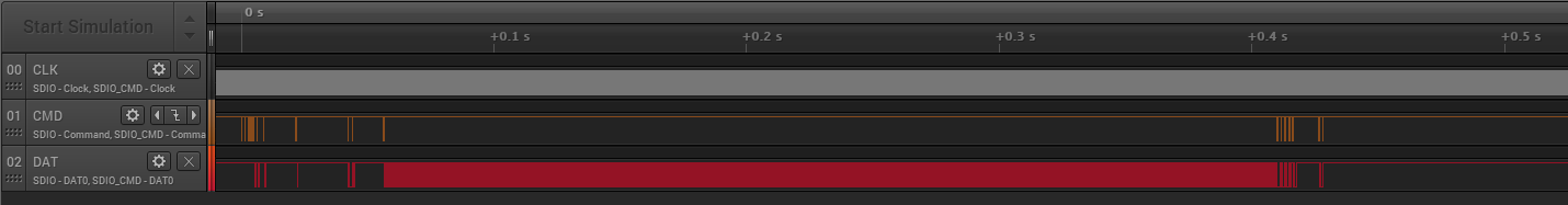
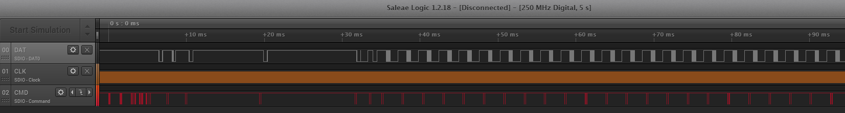
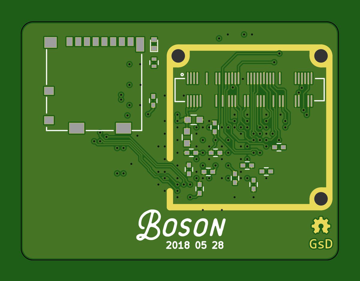
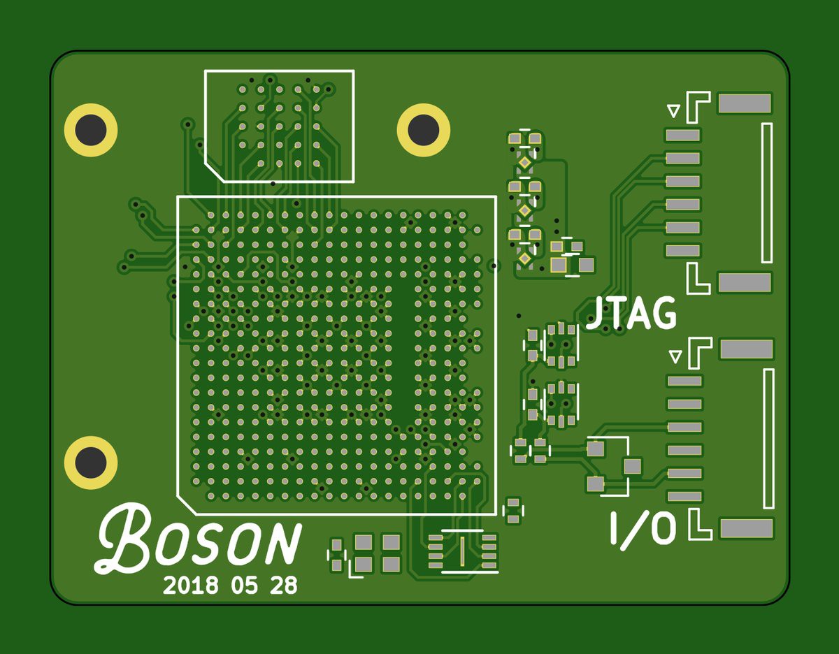
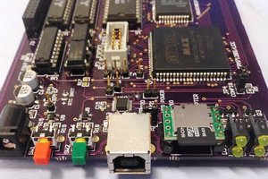
This project is a miniature FPGA based PCB to capture and save images from a camera stream. The FPGA used in the lattice ECP5, the board has 64Mbit of RAM and 8Mbit of FLASH. It runs a RISCV CPU internally to handle the processor centric tasks (UART, state machine, FatFS), but has dedicated hardware to handle the video stream and communicate to the SD card using 4bit SD protocol.
The modules inside the FPGA follow the following bus diagram. They all make use of a common wishbone buses.

All bus connections are created by this project: https://github.com/olofk/wb_intercon. wb_intercon automates the creation of muxes and arbiters required to connect various wishbone components including multiple masters.
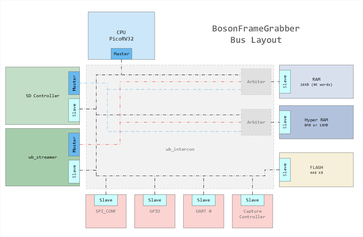 All the components make use of a common wishbone bus. There are 3 masters that enable data-flow through the device without requiring the CPU. Basically these are simple DMA controllers.
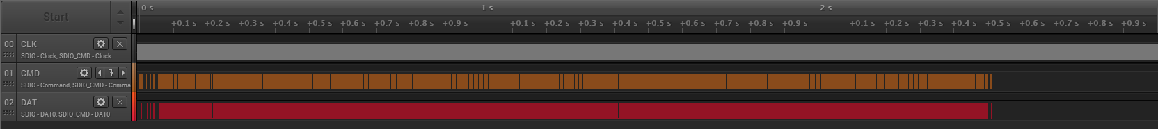


 tomcircuit
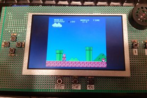
 Jon Thomasson
 Tobias Rathje
 Andrew Henderson
that's really cool!
lots of questions..
1. what's the power consumption;
2. do you plan to add a display to output the realtime image?