 Ken Yap
Background
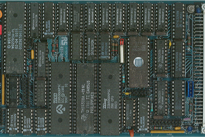
Some years ago I recovered a couple of boards out of copiers in e-waste. One was still mounted in its aluminium chassis, with a power socket, power switch, RS-232 connector, and power transformer.
Inventory
There are:
Z80 CPU running at 4.9562 MHz
Z8430 counter timer chip
Z8440 SIO chip
2764 8kB EPROM (removed from socket and contents dumped to a file)
8kB static RAM
LSTTL glue chips
RS-232 interface chips
A LM339 quad comparator, suggesting some kind of analog input
7805, 7808, and 7908 regulator chips for +5, +8, and -8V supplies
6 darlington power driver transistors, 3 each of TIP130 and TIP135
A huge transformer with one winding supplying +5V for the processor and chips and another winding for the positive and negative power lines to the power transistors
Memory space
ROM space is from 0x0000 to 0x7fff. 27128 (16kB) EPROMs can be used without modification, 27256 (32kB) EPROMs can be used with one address line modification
RAM space is from 0x8000 to 0xffff. 32kB RAMs can be used by changing one bridge track to another on the board
I/O space
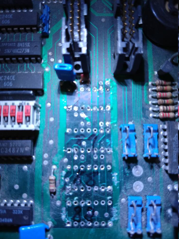
74LS138 1 of 8 decoder occupies 0x00 to 0x07. These ports are used, according to a disassembly of the ROM.
- O2 goes to 74HC273 CP
- O3 goes to 74LS04 then to drivers?
- O4 goes to ?, has out instructions but no track?
- O5, O6 go to 74HC240s 1G and 2/G
These seem to be for driving/reading the buffers in the middle of the board which connect to power transistors and sensors (switches?).
Z8440 SIO occupies 0x08 to 0x0f
Z8430 CTC occupies 0x10 to 0x17
SIO chip
The clock source for both channels of this is the system clock, divided by 32. This gives a baud rate of 9600.
Debugging
After a failed attempt to get the SIO working, I decided to start from basics and get a LED to light up. I wired up one between the output 0 of the 74LS138 and +5V with a current limiting resistor. Every time an IN or OUT instruction is directed to port 0, this should go low.
I wrote a short program to keep writing to port 0. It won't blink but should light up the LED a fraction of the time, for the period that the chip select is taken low by the OUT instruction. Unfortunately even this program failed to work. A probe with a voltmeter of the various ICs on the board showed fluctuating readings of Vcc on the highest numbered pin, and even fluctuating voltages of the order of tens of millivolts between GND pin and the power supply GND. This means that the connections to the chips and in particular the socketed ones are unreliable due to corrosion.
I could get out the digital scope but I've decided to cut my losses. There is another identical board that I could work on, but even if I get that to work, and work reliably as it's probably equally corroded, the resources on the board are not great. For I/O it only has a dual SIO, and parallel I/O comprises some 74LS240 latches in the middle section of the board driving power transistors. It's not much fun to get a serial interface working; maybe I could get Forth working on it, but what would I drive? Modern MCUs are so much more capable and easier to work with.
So I'm going to post this and then mark the project abandoned. That will free up mental energy to work on other projects.
 Keith
Keith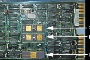
 jimshortz
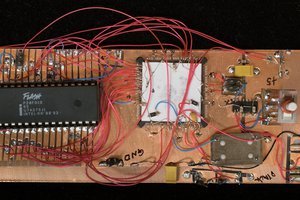
 Plasmode