 Tony
Tony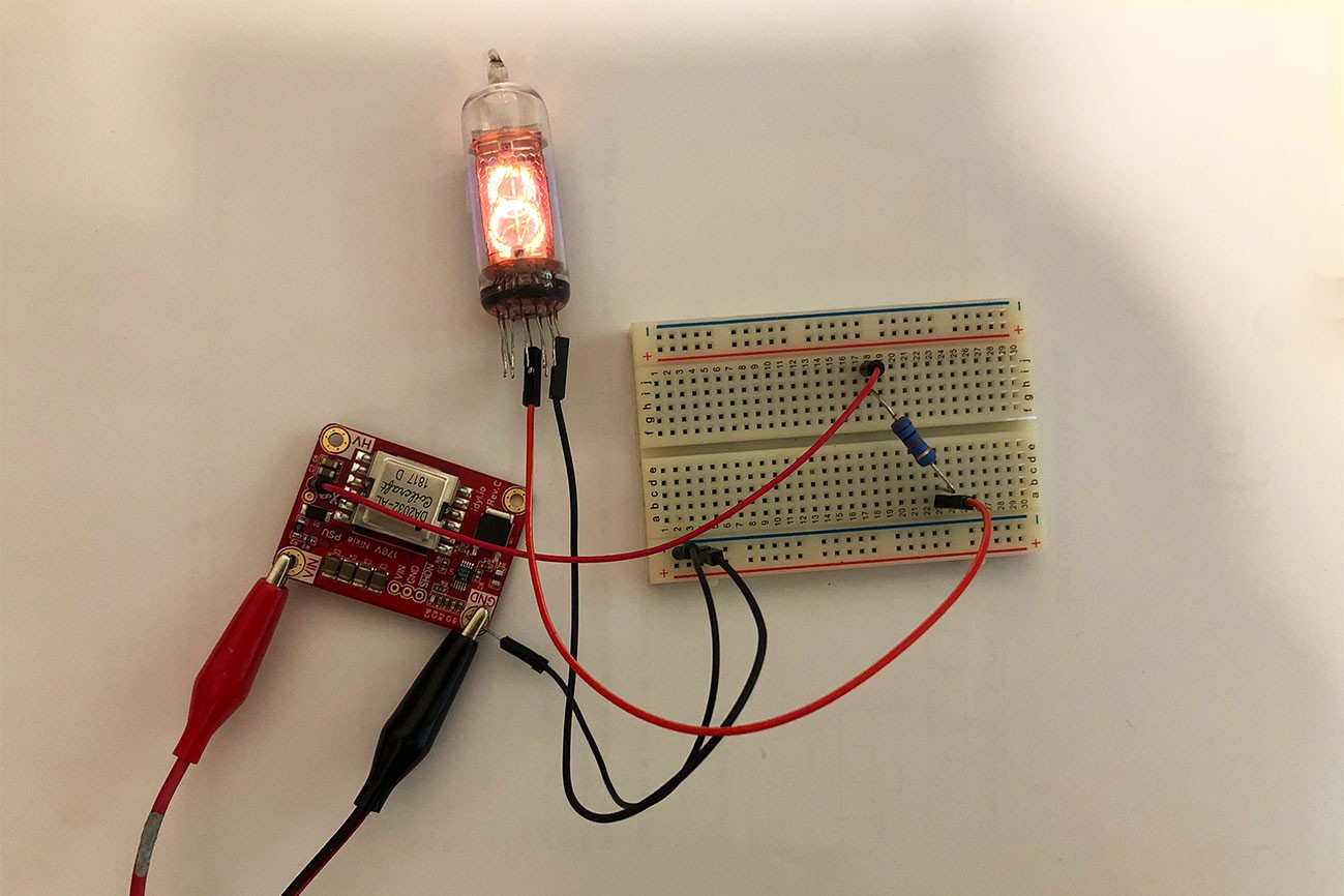
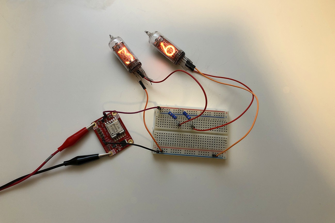
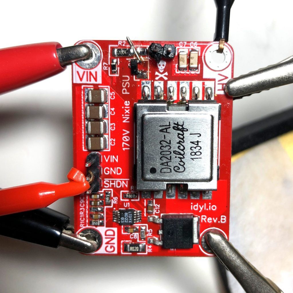
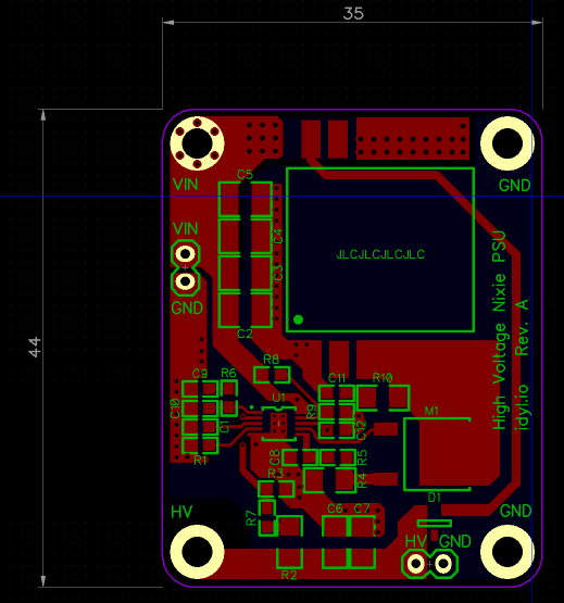
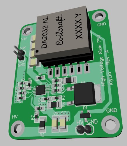
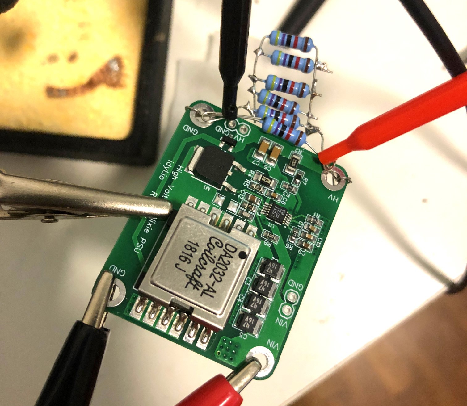
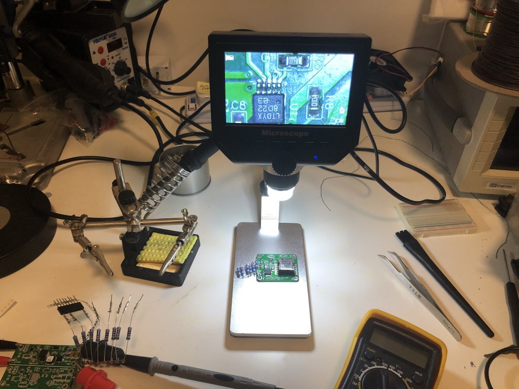
These pages describe in great details how I built a reliable and efficient high voltage nixie power supply -showcased above-; from the idea to selling it!
Be sure to read project logs!
- Part 1: Idea
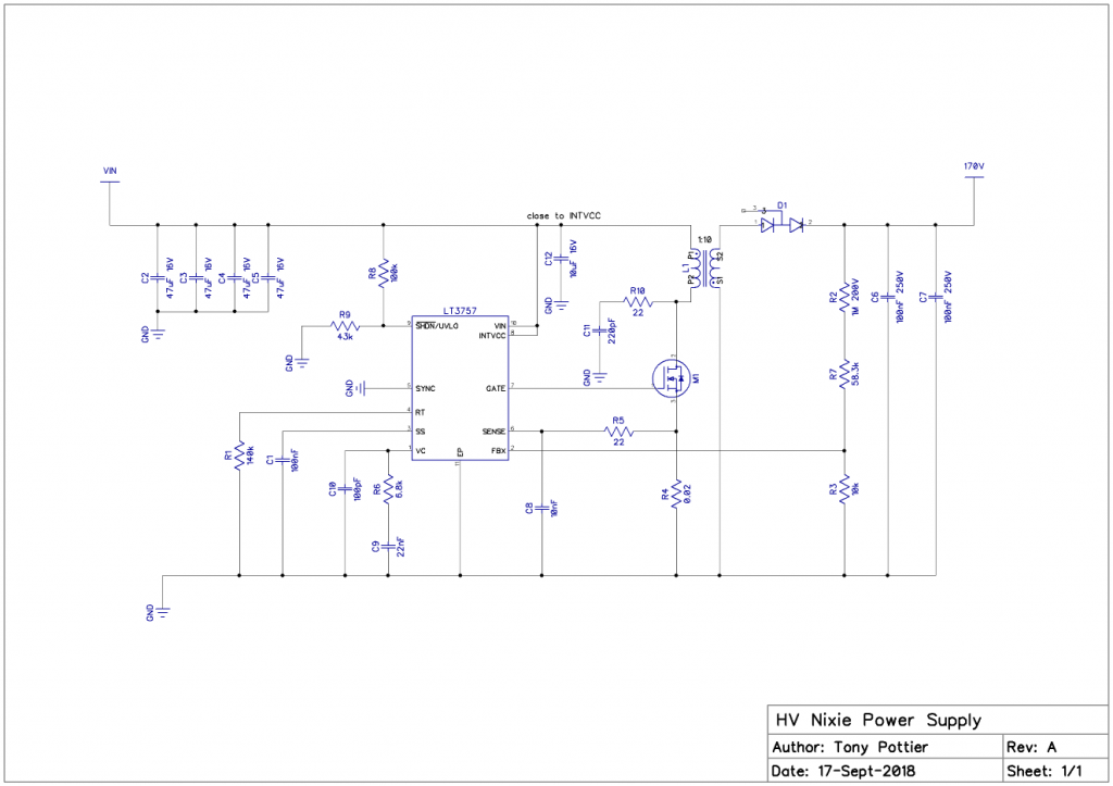
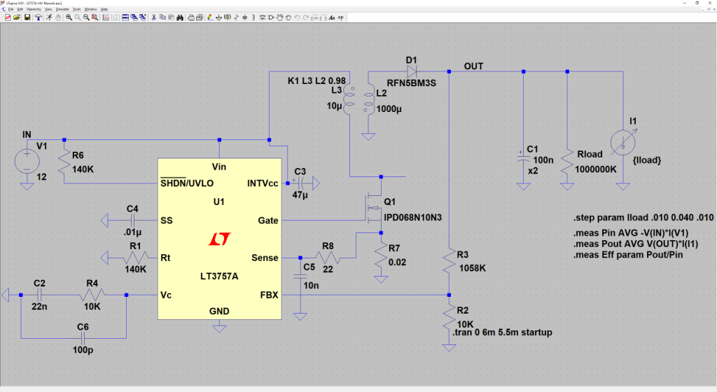
- Part 2: Design & Simulation
- Part 3: Making a prototype
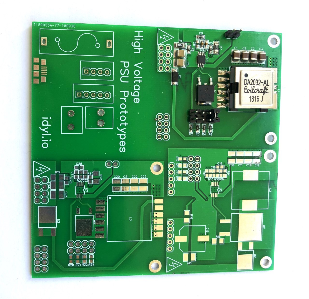
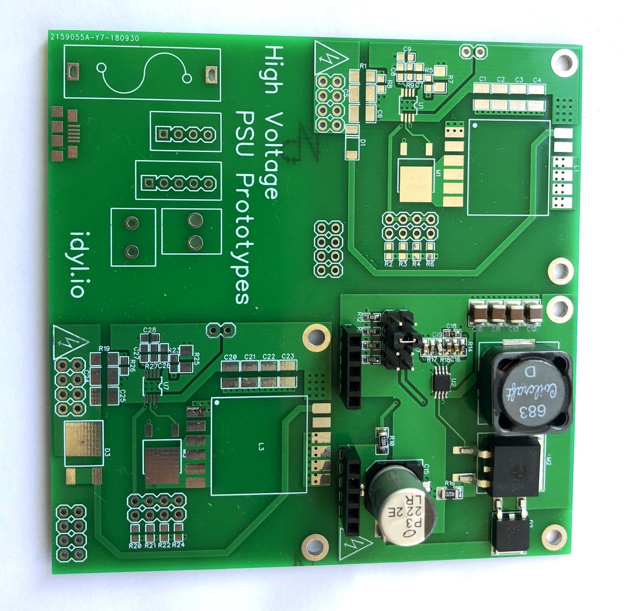
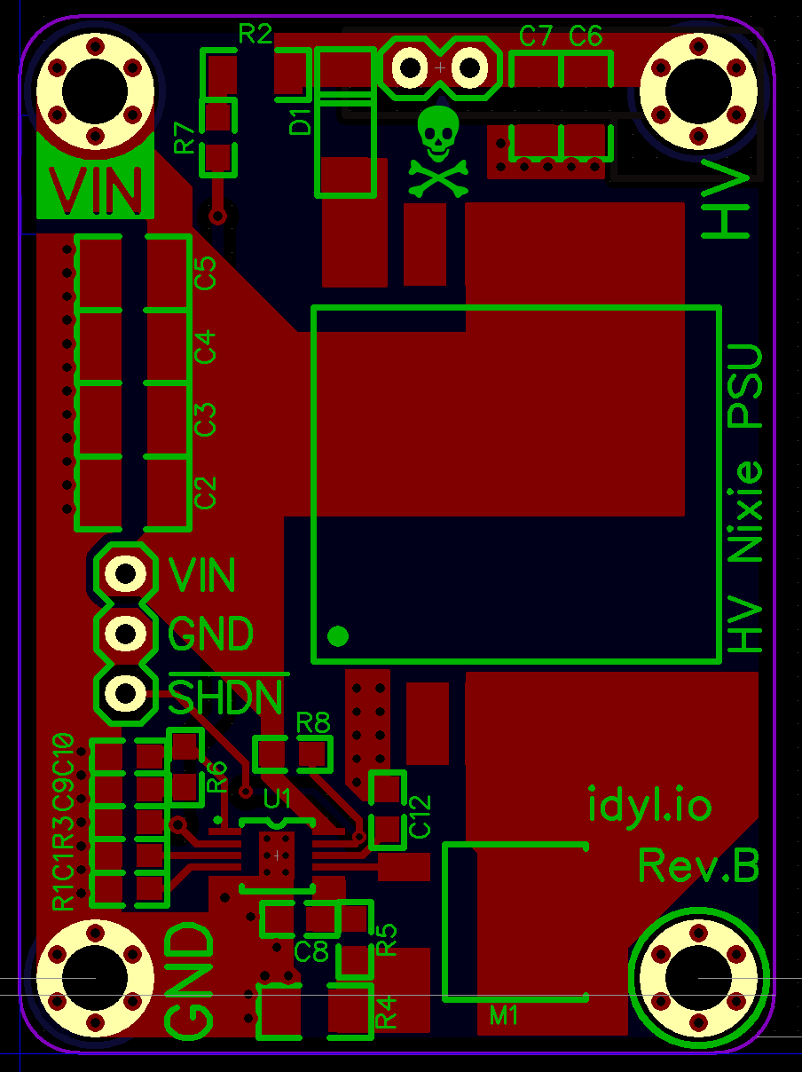
- Part 4: More prototypes!
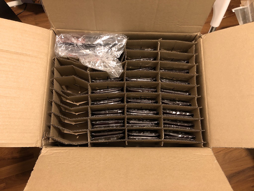
- Part 5: Sending for Assembly
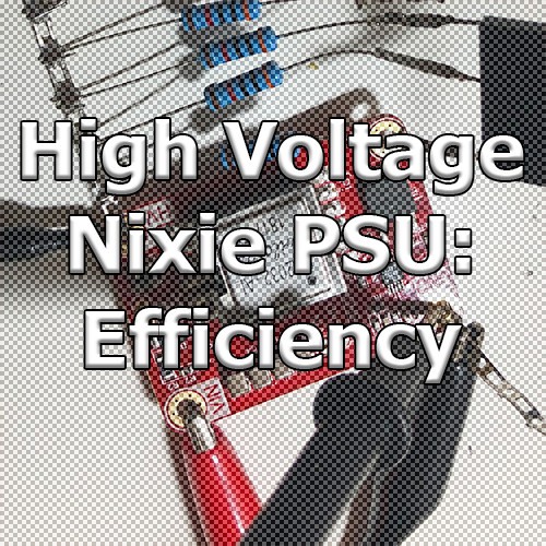
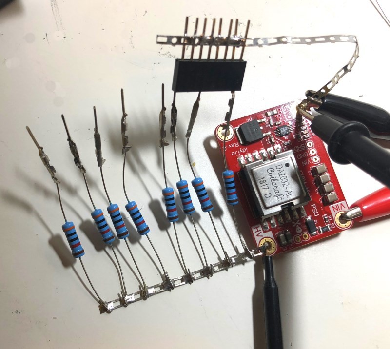
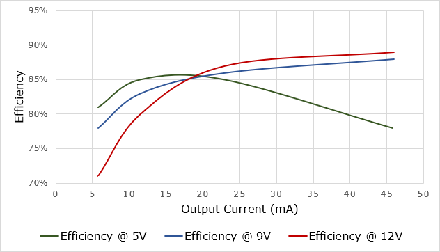
- Part 6: Efficiency
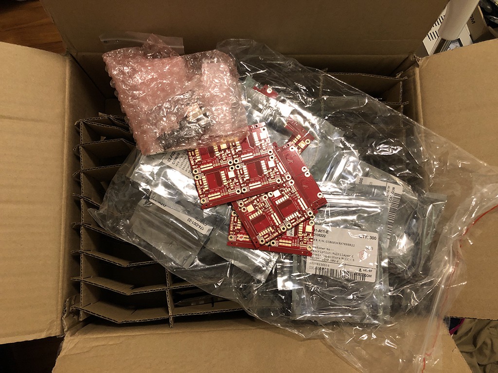
- Part 7: Production Run
- Part 8: Selling & Conclusion


 ivorivetta
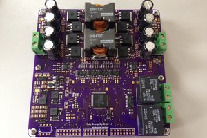
 Nathaniel VerLee
 c.Invent
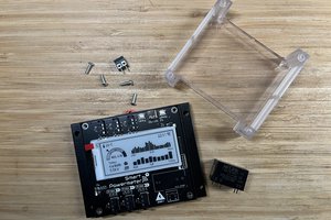
 Jon
Jon
Thanks for spending the time documenting this. It was very interesting and informative.