 Amos
AmosI am quite happy with my latest PCBs for this project (thanks JLCPCB!) although they do have some issues. The matte black boards look particularly sexy, although flux residue can be a bit of an issue if not cleaned up.
I thought it'd be nice to give you a brief tour of the board and talk about some of the things I will most likely be changing for the next revision. The next revision will be some time off, but I am building a wishlist of things to change/add.
A Brief Tour
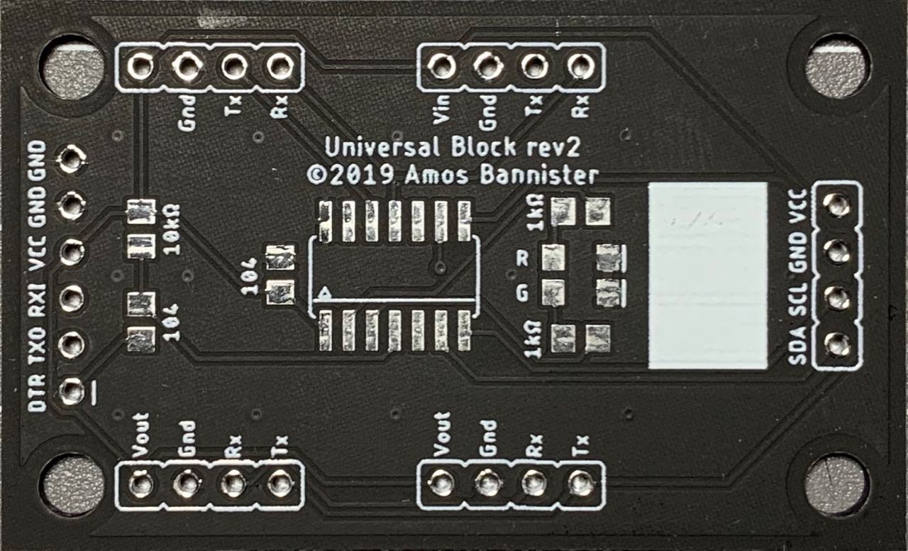
So let's have a quick look at the current boards:
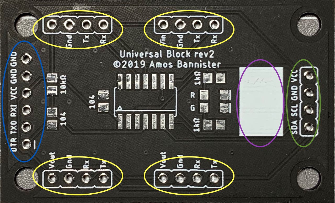
First of all, please ignore the missing Vin at the top left of the board - somehow I managed to delete it before I generated the Gerbers. 8^/
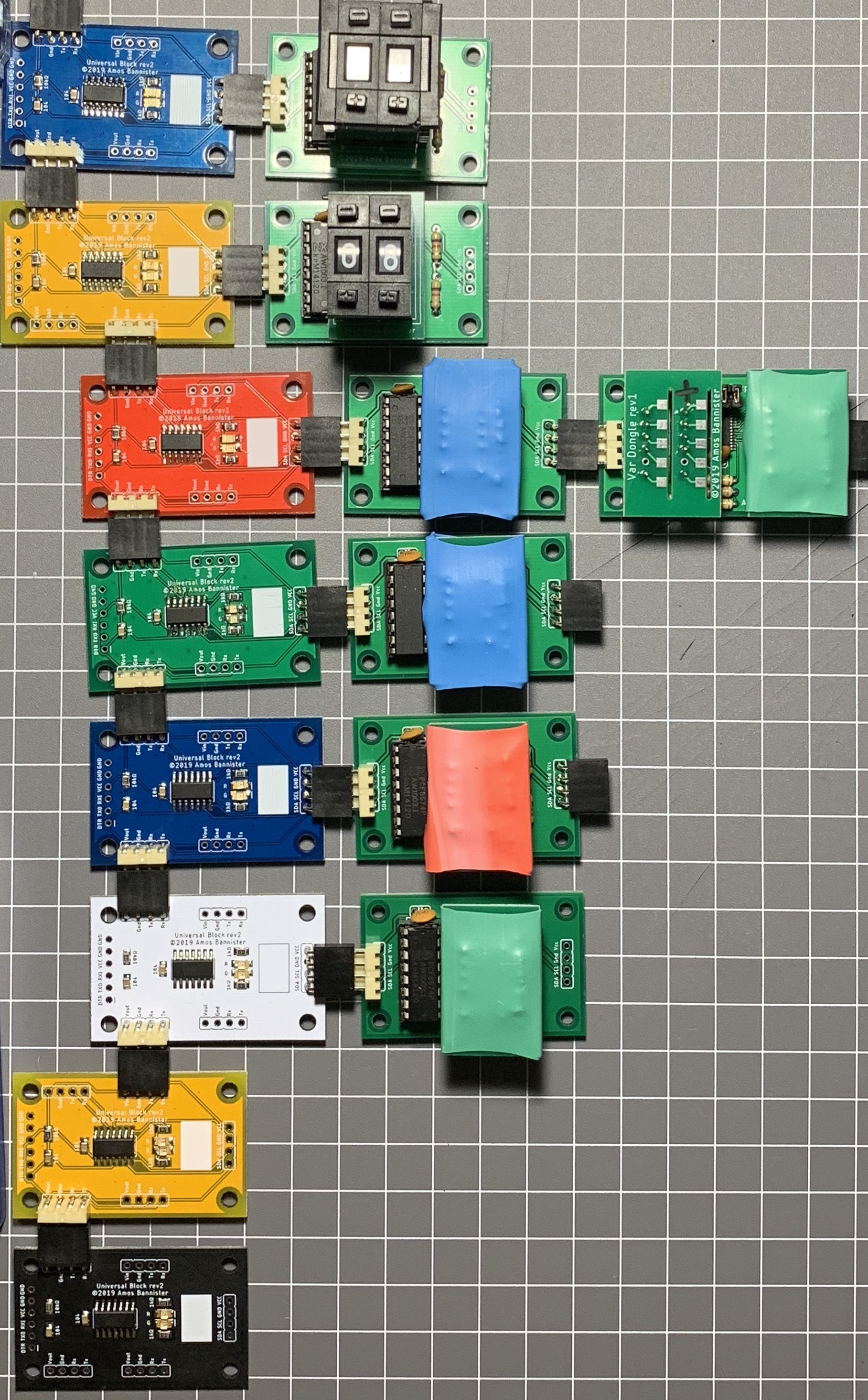
The board is designed to be somewhat flexible, with two incoming serial connections, and two outgoing serial connections. (Highlighted in yellow above.) Both of the ports at the top of the board are connected, as are the two ports at the bottom. This means I can choose to solder the 4-pin connectors in either position, which lets me create blocks that "indent" the code. This can be seen in my favourite demo program (which calculates the Fibonacci sequence) where the yellow LOOP block makes sure the loop contents are nicely indented and the END LOOP block un-indents the code.
At the right end of the board is a four pin port which is used to connect to other modules. Currently I am using this for value and expression blocks. The port uses I2C, so theoretically any I2C module could be plugged in. (With the appropriate code modifications of course.) That means it might be possible to plug an OLED display directly into a board, or even sensor modules such as temperature, light, or sound sensors, opening up a whole world of new possibilities.
The last port on the board is a programming header. (Circled in blue above) I built a pogo-pin adapter with a USB to FTDI module to program the blocks via this port, and it all seems to work fine.
Lastly, there is a white rectangle at the back of the board where I can label the board's function if required. At the moment I have been able to keep each colour to a a different programming construct and thinking about it, this label might not be needed. For example, yellow boards are being used for LOOP/END LOOP and I will build some yellow variable boards, but the placement of the input/output ports will be enough to distinguish variables from loops.
Other things to note about the boards: There is no power regulation on the board. This was not an oversight - it is by design. The boards draw their power from the input port and the master controller (currently an Arduino Uno, but soon to be a separate custom board) is used to handle the regulation of power. This has allowed me to reduce the parts count and make the boards a bit cheaper to make.
There are two indicator LEDs - one red and one green. The boards can use these to indicate their current execution states, or if they have an error.
And apart from that there is not much else to these boards. K.I.S.S.
Some Issues
Alas, it is not all smooth sailing however...
Flashing the Bootloader
Apart from the missing Vin label, there are a couple of other issues with the board. Starting with the biggie - I forgot to consider how I would flash the bootloader. Oops! While I have the FTDI header, that is not used when flashing the bootloader and setting fuses on the chip. I did manage to get it all working, but it is a bit of a bodge.
To flash a bootloader you need access to an ICSP port. On ATTiny (and ATMega) chips, that means connecting to VCC and Ground (got both of them on the serial ports and the I2C port), MISO, MOSI and SCK (those are TX Out, SCL on the I2C port and RX Out) and the RESET pin. There is a RESET on the FTDI header, but that is connected to the RESET pin via a capacitor, and the ICSP protocol doesn't like that idea. 8^(
I was able to flash the bootloader by connecting the the five broken out pins (basically the outgoing serial port and the SCL pin on the I2C port) and holding a jumper lead on the RESET pin of the ATTiny841 chip. If I slip, the flashing fails, but no damage is done, I just have to try again with steadier hands. As I said, a bit of a bodge, but it is doable.
A minimal fix for this would be to add a breakout for the RESET pin. A slightly better idea might be to include solder pats for an ICSP header underneath the board - that's prolly what I will end up doing.
Wandering LEDs
Another issue relates to the LEDs. Somehow when I was moving components around I moved the LEDs too close to one another. There is enough space that I can solder them without shorting, but it is a bit close for my comfort. I know exactly when I made this mistake and I own it. I just have to be careful of the LEDs shifting while soldering.
Another issue with the placement of the LEDs is where on the board they are. I really didn't give any thought. On the previous revision of the board, the LED (a single, bi-colour jobbie) was plonked down between the two incoming serial ports. That worked well enough, so why did I move it/them? I honestly don't know. I chose to use two discreet LEDs for... reasons... and having made that decision I figured they would fit as nicely between the two ports, so I stuck them behind the ATTiny. Not my brightest idea to be honest.
I think the LEDs would be happier if they were placed at the front of the board, next to the FTDI header. This would also allow me to make some interesting additions to the next revision without causing issues - but more on that idea later...
Future Changes
So I have a small list of changes that should be made for the next revision. Fixing the silkscreen is easy enough. As is moving the LEDs to a smarter location. Adding bare solder pads for an ICSP program header is a solid idea as well. I could then use another pogo-pin jig to flash the boards. If I want to get real fancy I could even make an automated tester/programmer like Unexpected Maker did for his TinyPICO boards! 8^)
The value of extra GPIO pins?
I have come to realise that most of my programming constructs require at least one value to make sense. For example, the variable assignment blocks (Blue, Red and Green in the program above) all need a value and an optional expression to function at all. A loop block needs to know how many times to loop, so that needs a value (or an expression) to function properly. Th output block needs to know what to output, so it also needs a value block to function. This all made me realise that I should probably integrate the value module with the program block. Now that I am using the ATTiny, there is plenty of space on the board for the value modules headers.
Adding a value module to the program board will require a bit of extra thought however. The ATTiny doesn't have enough spare pins for a full value module. For that I need at least eight spare GPIO, or four if I use Charlieplexing. I only have three GPIO pins spare unfortunately. Unless I use the Reset pin as a GPIO, but I think that would require some extra circuitry to allow flashing/programming.
An option might be to use an ATMega328PB. This will give me more than enough GPIO pins, while retaining the dual serial ports of the ATTiny841. As an added bonus it will also give me more memory to play with, which might make connecting to other Arduino-compatible sensors and modules easier...
What about the LEDs?
The LEDs should move, in fact they will have to move if I add the value module to the board. So where exactly should the LEDs move to? These blocks will eventually be housed in cases, so the LEDs should be in a consistent location to make the case design easier. They also need to be in a prominent, viable location. Top-left? Centre-Left? Bottom-Left? Between the input ports? I don't know just yet - this will take a bit of thought...
Discussions
Become a Hackaday.io Member
Create an account to leave a comment. Already have an account? Log In.