Amos
Amos-
Playing about with LEDs
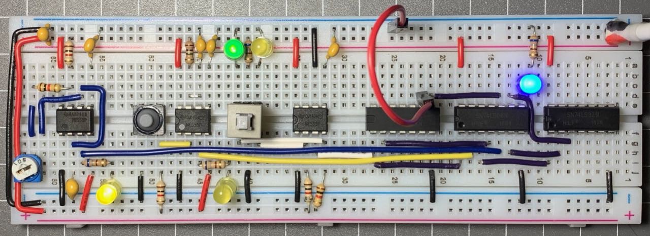
02/09/2019 at 09:41 • 0 commentsThe extra wire I needed finally arrived last week, but unfortunately I have been too busy with other things to work on this (or any other) project. 8^( I did spend a little time on the computer today though - I made up a bunch of LEDs with integrated resistors and tweaked the wiring of the registers so they work a bit better.
I wasn't particularly happy with how Ben drives LEDs directly from the 74LS chips with no current-limiting resistors. Not only is this "a bad thing" IMHO, but the blue LEDs can be particularly bright when driven so hard. Adding resistors while keeping close to Ben's layout is kinda hard, so I tried out two possible solutions.
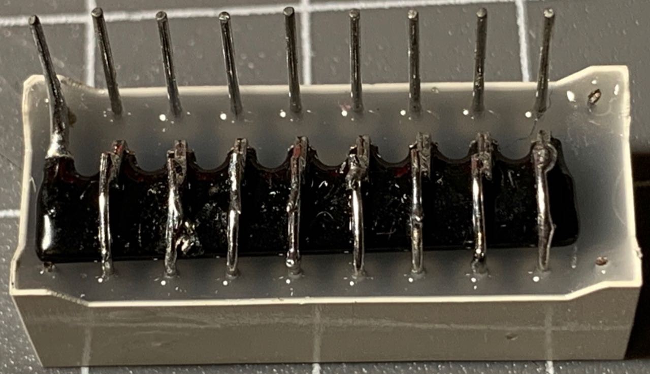
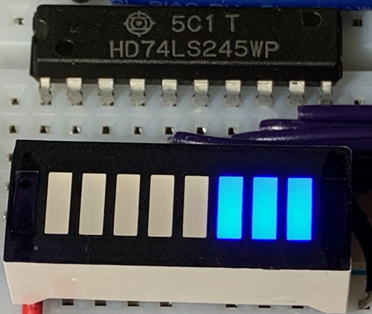
Option one was to modify some 10-segment LED bar graph displays with a resistor array. Bending the pins on one side of an LED display over and soldering them to the pins of a resistor array allowed me to turn the display into a SIL device. This is ideal for plugging into the pins of a 74LS245 to display the current value. Unfortunately, not all the blinky lights on the computer are so nicely laid out, so a SIL LED bar graph would only be useful in a limited number of places. Plus, while I do like the look of the LED bar graph displays, I think the retro-ness of 5mm LEDs suits this project better.
![]()
![]()
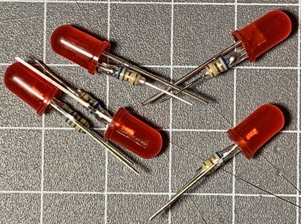
The second option was to solder resistors to the legs of LEDs. I managed to find some nice, tiny 1/6 watt resistors, so I decided to try using these and I think they turned out kinda okay. With these babies, I can just plug them in where Ben had his LEDs and they are not only less bright, but they should help protect the ICs by drawing less current.
![]()
And here's a very short video showing both LED solutions. The red LEDs appear a bit dim, especially the one of the right which is not pointing straight up here, but they are not really so dim in person. I quite like the look of the 5mm LEDs, so the rest of the computer will use these LEDs with in-line resistors.
-
My EEPROM programmer is alive!
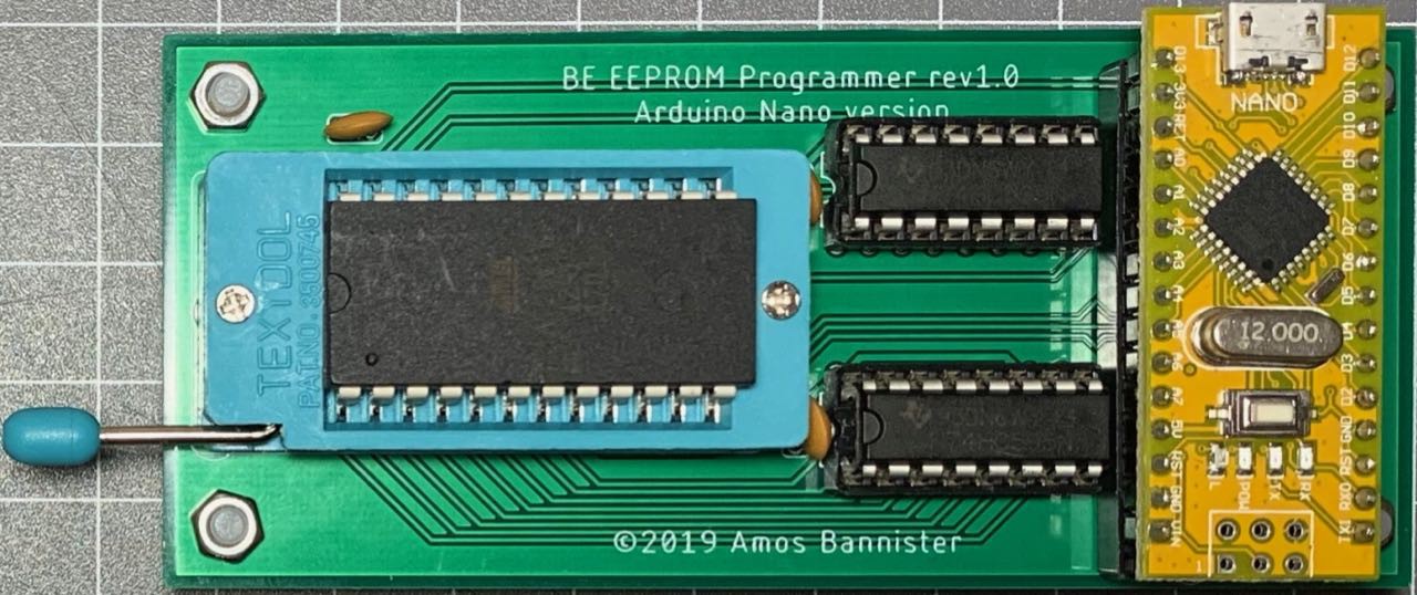
01/31/2019 at 10:06 • 0 commentsWhile waiting for more solid core wire so I can continue layout out the breadboards, I decided to build the EEPROM programmer so I could get a jump on burins the EEPROMs for the computer.
Although I am sticking to breadboards for the first iteration of my TTL computer, I did make one concession - the EEPROM programmer. There are several reasons why I chose this route. Firstly, there are just too many wires and it would be hard to get the wiring neat enough to satisfy me. Secondly, I did not like the idea of stuffing the 28C16s into and ripping them out of a breadboard multiple times like Ben Eater does in his videos - especially with the power constantly on! Finally, I do have other uses in mind for the programmer, so I wanted something a bit more robust...
I recently ordered a bunch of PCBs from JLCPCB for my Tangible Computing project, so I slipped an extra board into the order. I used a ZIF socket for the EEPROM and plugged the Arduino Nano in using a 32 pin socket (with two pins removed) so I can re-use the Nano if I want. The board worked first try and with a little modification to Ben's code I was even able to dump the contents of a 2732 EPROM I want to clone for another project, then flash a 28C16 with the contents. Awesome stuff! I am going to have fun with this. My next task is to write some better control software - something a bit more generic than Ben's software, which can be used for other upcoming projects.
![]()
-
Trouble with the registers
01/10/2019 at 11:03 • 1 commentGrrr! I spent today tidying up some wiring on my A and B registers and building the Instruction Register. Everything seemed to be working fine until the B register started acting up. Reading data from the bus is way, but when I enable to the output latch, not all the bits get put on the bus properly. I bit of poking and prodding at the wiring and sometimes (but not always) the data will appear. I know it isn't a power problem - I have checked the power distribution and it is nice and stable across the boards I have connected so far.
The culprit is most likely the wiring. I have been unhappy with one of the spools of hookup wire I have - the wire is difficult to work with and tends to break too easily. I need to toss the spool and replace the wiring, but that is not so easy. Where I live it takes around a week to get anything via mail order (even longer if it is from overseas) and there are no local electronics stores I can turn to. Plus I'm going away next week... In the meantime I will use a different colour (I like to colour code my wiring and I don't have any spare colours (yet)) to confirm that the wire is the problem and replace it (again) when I am able to get some new spools of hookup wire.
-
The clock module
01/06/2019 at 11:15 • 0 commentsThe first module I built for this project was the clock. With the exception of some LEDs, I have followed Ben's clock design as closely as possible. There are three 555 timers, set up as astable, monostable and bistable timers. The astable timer is used for the regular clock pulse, the monostable timer is for a manually triggered lock pulse and the bistable timer is used to select between the free-running timer or the manually triggered pulse. The logic chips (74LS04 Hex Inverter, 74LS08 Quad And, and 74LS32 Quad Or) are used to combine the signals from the three 555 timers, plus a HALT signal (the red fly lead just right of centre in the picture below) to generate the final clock signal. A schematic for this clock can be found on Ben's site. (Note: For this project, I will not be including circuit diagrams, instead I will link the Ben's site where he has diagrams and links to all his YouTube videos.)
![]()
The only real modification here is the inclusion of several indicator LEDs, so I can see what is happening. (Plus I love blinkenlights!) The green and yellow LEDs above the switch indicate whether the clock is in free-run mode (green) or manual trigger (yellow). The yellow LEDs on the bottom rail just show the output of the two clock timers.
While I think the module is a bit too complex for what it is supposed to be, I can understand that Ben is not designing an optimal CPU, rather he is using this as a way to teach people about 555 timers and logic circuits. I have already (half) designed a new clock for my next CPU project, and this clock will be much simpler, containing only a single 555 timer. I will push the handling of the HALT signal to the CPU-proper, so the clock will be just a clock - no complex logic dealing with combining signals, inverting signals or handling HALT states. My v2 clock will be as simple as possible.
-
Some thoughts on going from breadboards to PCBs
12/29/2018 at 11:23 • 4 commentsAs I complete each module of the computer, I like to revisit Ben's videos both to make sure I haven't missed anything and also to see what I can learn from the design choices made. Now that I am starting to design PCBs for each module, I am also finding it important to check later videos for any additions or modifications Ben makes to the circuits - there'd be nothing worse than "finishing" the PCBs and discovering that I'd missed an important change to the layout. Like the clock's inverted clock signal, which is used in the control logic module. Not really a problem - I have watched the series of videos a number of times bu I want to make sure I don't miss anything important on the PCBs.
While integrating later additions into my PCB designs is not a big problem, I am facing a moment of writer's block when it comes to laying out the PCBs and their interconnections. I would like to keep things affordable, so I am aiming for no larger than 100mm x 100mm (so I can get cheap PCBs made) and I'd kinda like to keep the layout somewhat similar to Ben's final design, with modules on either side of a data bus. But what to do about the control signals? I guess a control bus would make sense. I am picturing a control + data bus down the middle of the layout, with separate modules plugging into either side of this bus. So we're talking 8 data lines, 16 control lines, power and ground, clock, !clock (for only one module), halt, and the carry and zero flags. That's 31 lines, round it up to 32 for good measure. Two 16-pin connectors per module would do the job.
Given my size constraints (100x100mm), if I could get each module to fit on a 50 x 100mm board, I could fit two modules per bus segment. So far so good. Of course, some modules connect directly with other modules - the two registers (A and B) connect directly to the ALU, bypassing the bus for example. So whatever size connectors makes sense for those interconnections can be used.
One minor annoyance is the register design. Registers A and B are identical, so that's easy, but the Instruction Register is slightly different. Being a cheapskate, I'd like to avoid paying for a separate PCB design, so I need to figure out a way of modifying the design so the one PCB can server both register types, perhaps selectable by a jumper?
As I continue this build process, I am also taking notes for my next design. Ben's design choices have been made for a specific purpose - explaining how to design a CPU. As such, not all of his design choices are necessarily ideal. I think his clock is over-engineered for example - three 555 timers and thee logic chips just to implement a clock? When I redesign, I will choose a simpler clock design. I still want to keep the adjustable clock rate and single-step mode, but this can should be achievable with a single 555, and the only logic chips needed would be for the Halt and inverted signal - if these are really needed. (Well, Halt is needed, but does it belong in the clock circuit, or elsewhere?)Another design choice I will make with my own design, is separating the CPU functions from the general computer functions. Ben's design merges everything into one big design, but I'd like to have separate CPU, memory and input/output sections. I will also need to include separate address and data busses (external) for memory access and a larger address space is also a given. Do I need a separate flags register? Should the ALU be hard-wired directly to A and B registers, or is there a better design? (I'm guessing there is a better (and more versatile) way to implement the ALU and registers - if i add more registers, I should be able to use them with the ALU too, right?)
I'm okay with Ben's microcode ROM design, however the replication of instructions for each combination of zero and carry flags is a bit problematic - what if there are more flags and conditionals added? I will need to explore a better way of implementing this. There's also something about his output module that I am not entirely happy with, but I can't pinpoint what it is just now.
Anyway, I just wanted to get some (ramble) thoughts down before I forget them. ;^)
-
Some background first...
12/24/2018 at 13:18 • 0 commentsOver 30 years ago I took a computer science course that had an awesome textbook. (I can't recall the title of the book, but when I find it I will update this.) The book had a section on CPUs and how they work and at the time I wanted to try to design my own CPU using discrete components. I got as far as sketching out preliminary designs on paper and some proof-of-concept test modules, but a quick tally of the components required for a full build meant that the project would have been prohibitively expensive for me at the time. But I always wanted to return to this project... One day...
Sometime in mid 2018 I stumbled across a series of YouTube videos by Ben Eater where he shows how to design and build a CPU using 74xx TTL chips. Electronic components and chips are so much cheaper these days that such a computer is within reach of my (limited) budget. Finally I could do something approaching my original CPU idea.
My plans for this project are to build Ben's design (reasonably faithfully) on breadboards, then transfer the design to PCBs. I have already stockpiled most of the components (I need some more breadboards, as some of my stock was appropriated for some Arduino projects) and have the clock and two registers built. I will document what I have done so far in the next project log.
As I complete each module, I plan to create a PCB and immortalise the design in silicon. I have some crude layouts already, but I need to think about how the busses will work and how the modules will connect together before I get the first batch of PCBs etched.
When I complete this project, I desperately want to revisit my original idea of a fully discrete CPU. Or maybe a hybrid - use discrete components for some of the CPU and 74xx logic for the rest? I dunno yet, but I want to design a CPU form scratch - something different to Ben's implementation of Malvino's SAP computer, and prolly not a microcode-based CPU. We'll see how far I get. ;^)
Yet Another TTL Computer
Yet another TTL computer, inspired by Ben Eater's YouTube video series.