 Ted Yapo
A long time ago, I read somewhere about using 0.125" (~3mm) copper foil tape to create 50-Ohm traces on the back of single-sided copper clad board for quick RF prototypes. This width is very close to the usual 110-mil trace width you'd use on a PCB. Yesterday, I decided to try it out.
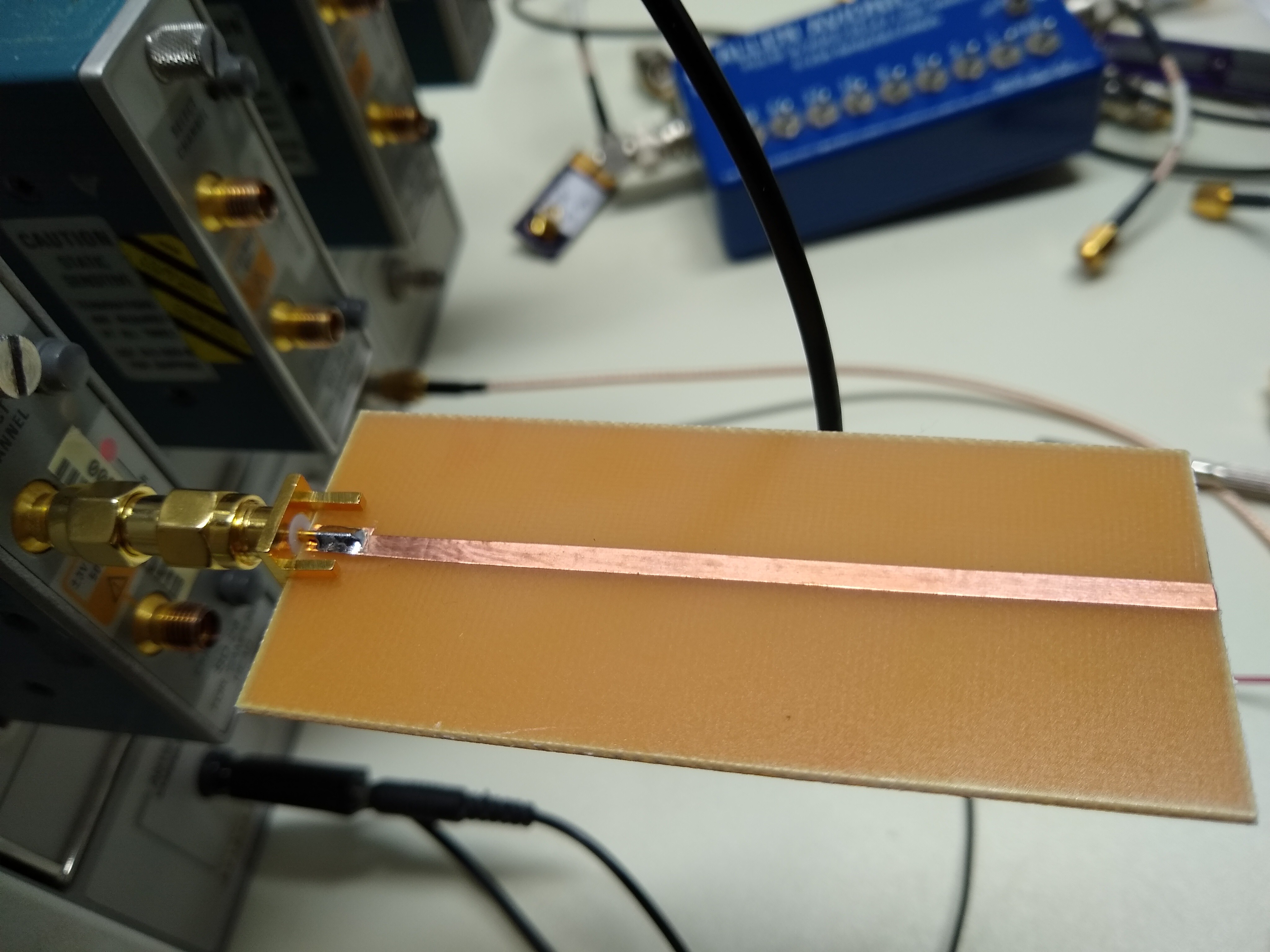
To run a trace, you just stick the tape to the PCB. The bottom of the PCB is un-etched solid copper which acts as the ground plane. I've done circuit prototypes this way before, but never really investigated the technique.
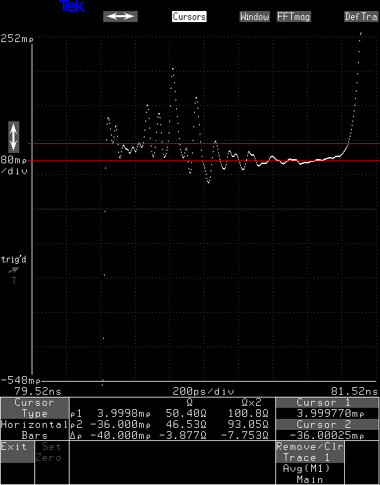
With the full 125-mil width, the impedance is a little low, reading around 46.5 Ohms. Don't worry if you find it difficult to interpret the trace. I found that I can locate what's what on the screen by touching the PCB trace with the tip of a screwdriver; the added capacitance shows up as a bump in the response. 46.5 ohms isn't bad - that's under 1.08 VSWR, and 29 dB return loss. You can also see how my lousy cheap M/M SMA adapter and board launch cause all sorts of bumps. Quality microwave connectors are expensive for a reason.
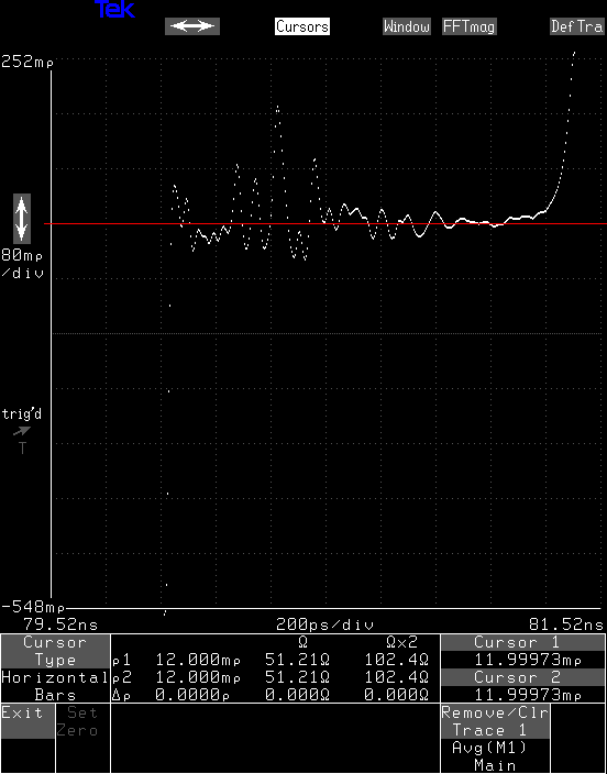
I tried cutting the trace down slightly (the image above is of the trimmed foil - you can see a little notch right after the BNC connector. I removed too much foil, and ended up at 51.2 Ohms. This is a little better at 1.03 VSWR and around 38 dB return loss. Whether this extra precision is worth the effort depends on what you're doing.
There's a lot more that would be interesting to look at - like loss, for instance - but being able to whip up some prototypes quickly without etching, milling, or waiting for PCB fab services sounds pretty appealing.
The problem, of course, is that this microstrip trace is really big. I wonder if I can find some thin single-sided copper clad that would bring down the trace width?
Discussions
Become a Hackaday.io Member
Create an account to leave a comment. Already have an account? Log In.
>I wonder if I can find some thin single-sided copper clad that would bring down the trace width?
I got a couple of very large sheets (like 11"x17") 17 mils single sided PCB way back in my University days from the old Active Surplus in Toronto. Also used to get scrap PCB there.
I would use as thin a trace as the SMB pin as the breakout as the round pin by itself is probably at 50 ohms. The breakout would have a triangular wedge to the copper trace which would smooth out the transition to final impedance even if it has a mismatch.
Are you sure? yes | no
@Ted Yapo If you start by taping kapton tape over the copper clad, and then tape a copper tape trace over the kapton, you will have much reduced geometry.
Are you sure? yes | no
yeah, that's a good idea! Kapton has an Er of around 3.0. It comes in different thicknesses, but you can get it up to 5 mil readily. A 50-Ohm trace on that would be 11.7 mils wide. You'd have to cut it down to thickness before applying it because you wouldn't want to cut the kapton (?), and then taping such a thin strip might be tough. Maybe you could make a jig to cut a precise thin width? This all ignores the adhesive thickness and properties, too.
an interesting idea. Maybe there's some other substrate that could be used - you can apply copper tape to both sides of a slab of something else entirely - maybe something resembling a real microwave substrate. Borosilicate glass? Or a few layers of kapton.
I wonder what the other properties of kapton are? Like the loss tangent?
Are you sure? yes | no
For reducing RF losses, you would want as wide a track as possible - skin effects and slightly less resistance.
Are you sure? yes | no
I wonder if a stack of double-edge razor blades with appropriate spacers in between could cut a bunch of thin copper foil traces at once?
Are you sure? yes | no
There were thinner copper tapes back in the old days for repairing PCB.
Are you sure? yes | no
I was thinking something along lines of laser cutter, for those who have it, and maybe it could be extended into a rapid prototyping technique on its own, alternating adhesive sheets, with cutouts, of kapton and coper foil, ending with kapton "solder mask"/solder paste stencil layer, but ... for this particular task, especially without laser cutter, could you just etch a trace in a length of tape, just like you etch a copper clad?
Are you sure? yes | no
BTW copper tape over kapton over existing ground plane on a PCB is my usual way of adding a high frequency power plane for mods.
They used to laugh at that as it would have lower impedance than a real multilayer board as there are no long vias or thin breakout tracks for decoupling caps or to the chip. If all else fails, I have a nice roll of 50 ohms microcoax.
Are you sure? yes | no