Ted Yapo
-
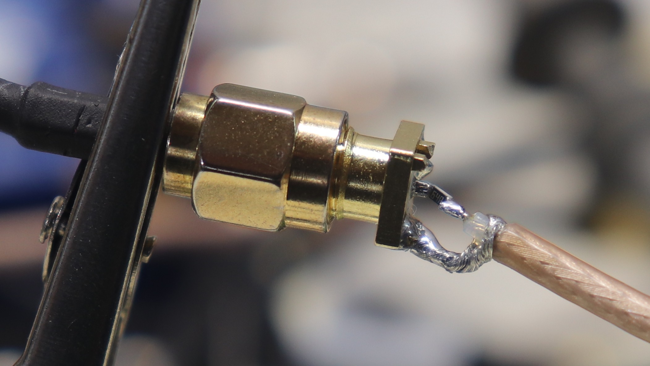
SMD Z0 Probe
05/04/2019 at 16:50 • 2 commentsIn the last log, I looked at a resistive (Z0) oscilloscope - and spectrum analyzer - probe I had been using for a while. That version used a small metal film through-hole resistor. To see how SMD parts would compare, I built and tested another version this morning. This would probably be a single-use probe soldered on a PCB, but the parts are cheap enough.
![]()
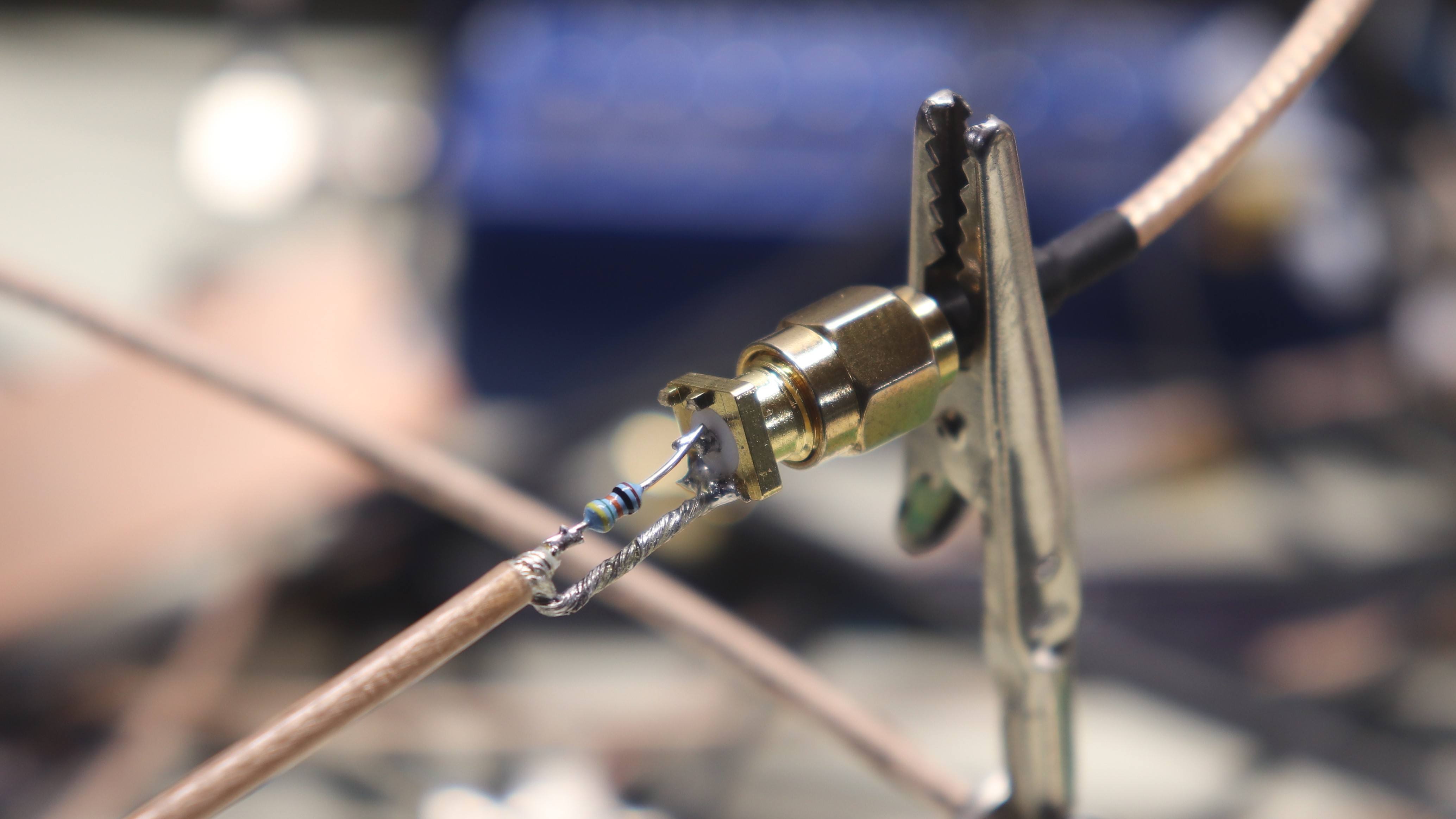
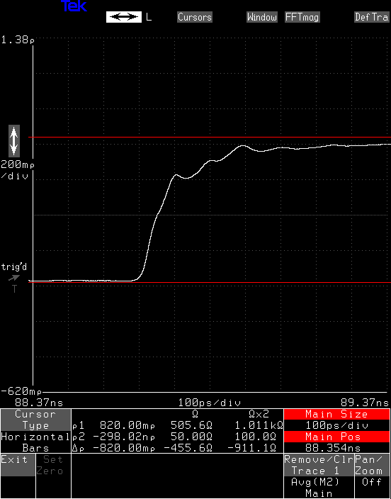
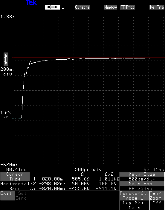
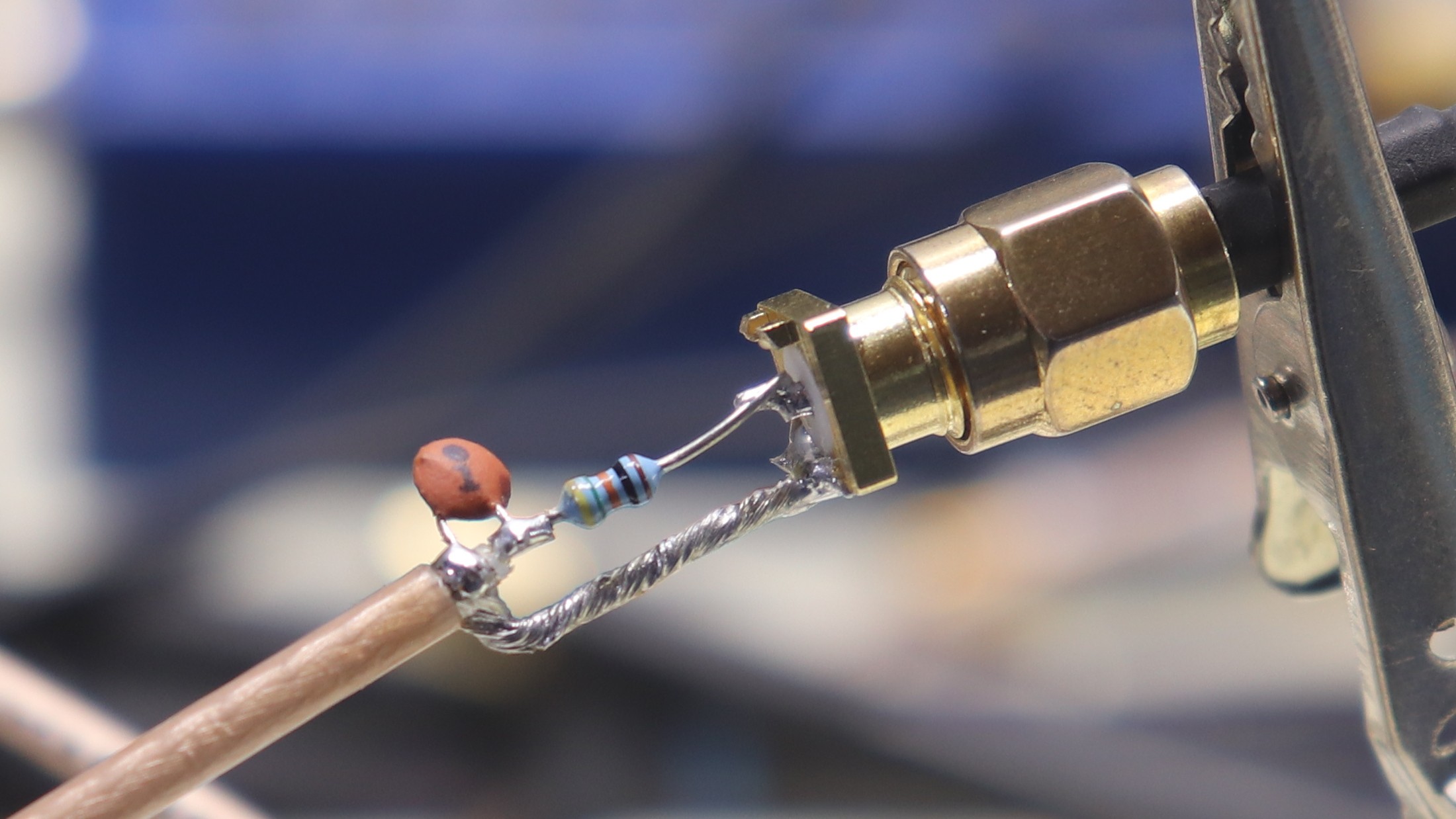
This version uses a 453-Ohm 0603 resistor for a 10:1 probe with an input impedance of around 500 Ohms. Specifically, this uses the cheapest resistor I could find, a Yaego RC0603FR-07453RL. I bought them from DigiKey, but search is broken on their site at the moment, so you get a Mouser link instead.
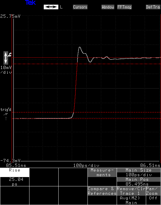
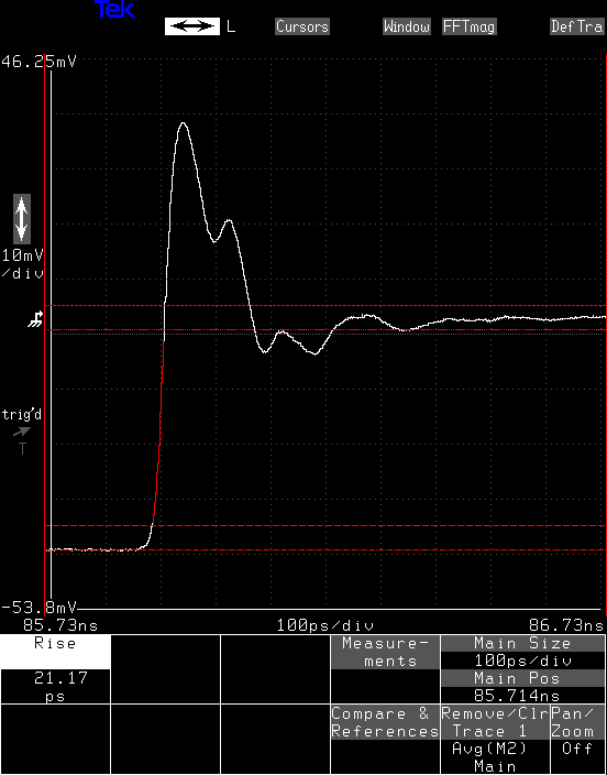
The response looks pretty good right away. The rise time is 25 ps, again, at the edge of what I can measure. There is a 20% overshoot, then a negative ripple that looks fairly well resolved by 100 ps. That indicates it might be a decent probe up to around 3.5 GHz.
![]()
Simulation
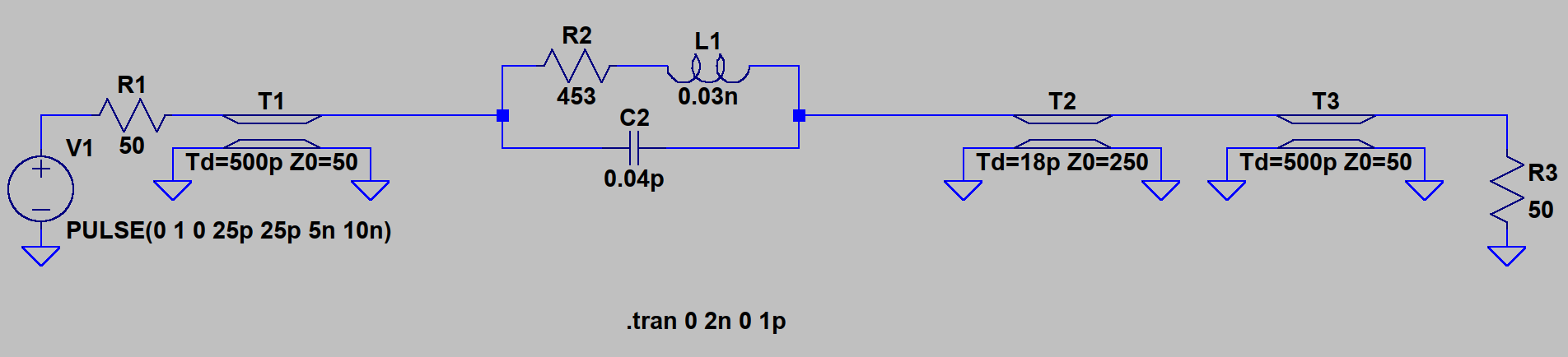
I took a wild shot at simulating this in LTspice. I looked up some typical package parasitics for 0603 resistors, and modeled the probe as a parallel-wire transmission line. Using 1 mm diameter as the conductor and 4 mm as the spacing, the impedance of such a parallel-wire structure is about 250 Ohms. At a length of 5.5 mm in air, this transmission line should have an electrical length of 18 ps. This is the model I ended up with:
![]()
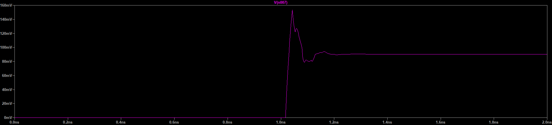
Hit with a 25 ps rise-time pulse, you get this response:
![]()
At least qualitatively, I can recognize the basic features of the response. There might be something to this approach.
Compensating Cap?
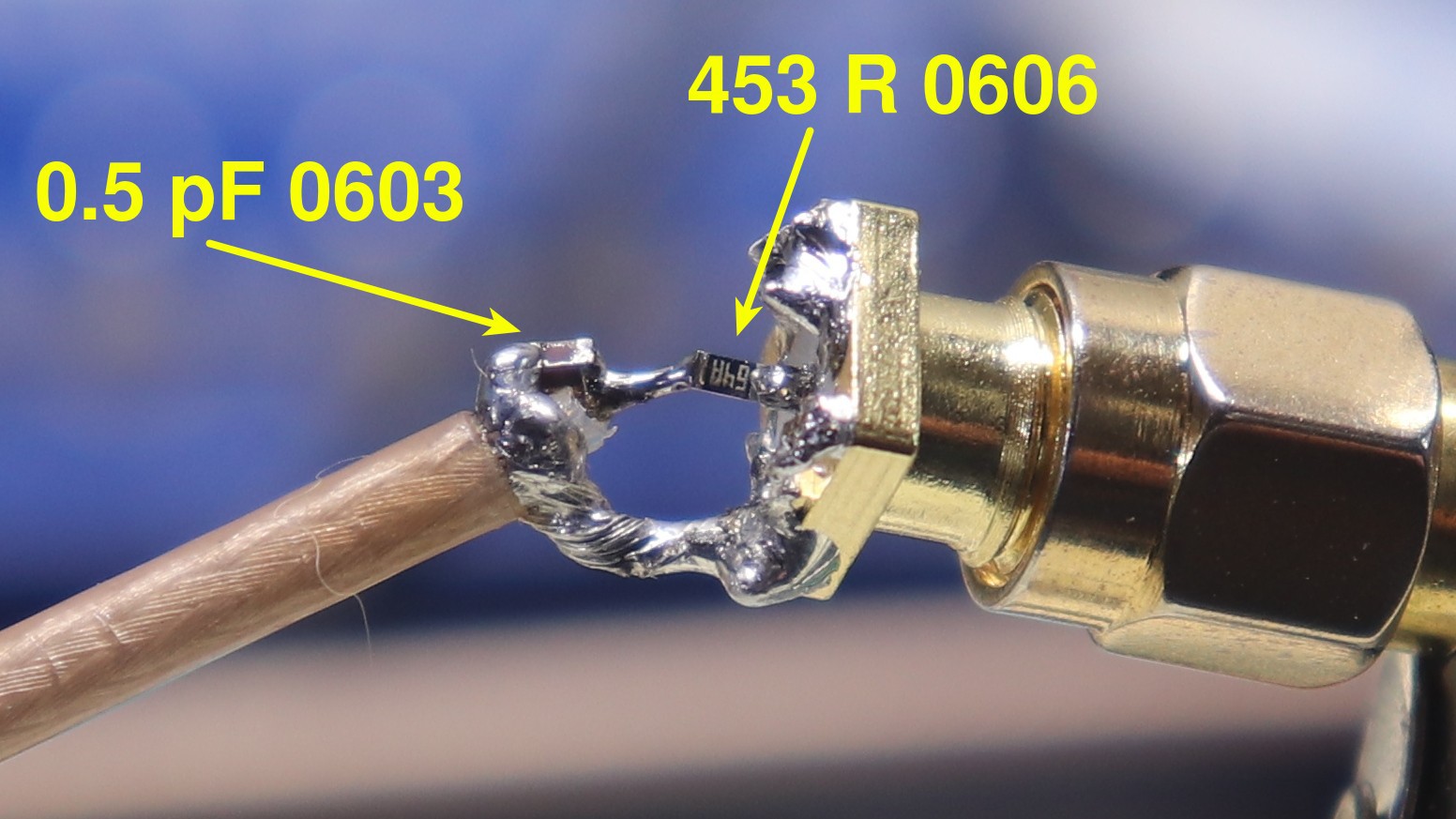
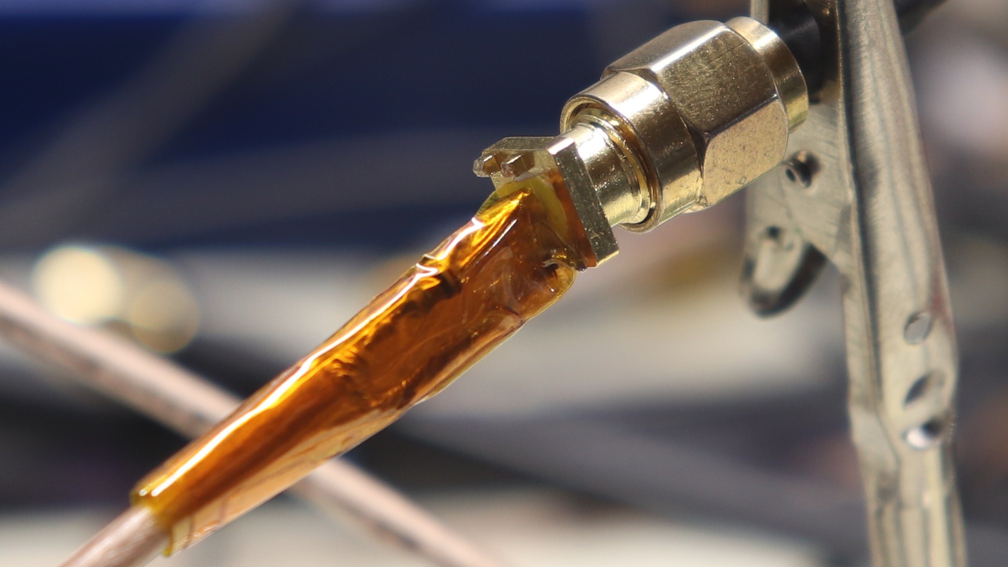
I found that applying just the right amount of compensating capacitance with my finger could flatten out overshoot and turn this into a 10 GHz probe. Then, I wondered if the same could be done with an SMD capacitor. The smallest one I had in stock was an 0603 0.5 pF, so I soldered it on there to see what would happen. I broke the solderable contacts off of three resistors doing this. SMD components are not meant to take much force.
![]()
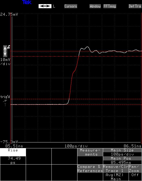
The result is definitely over-compensated: you can see the capacitive step. This also adds 50 ps to the rise time. Overall, not really an improvement. This is the sort of thing you do with PCB pads, not lumped-element components.
![]()
-
My (Old) Favorite Z0 Probe
05/04/2019 at 01:18 • 7 commentsI have often used a Z0 (resistive) probe in the past, especially for fast digital logic. This consists of nothing more than a resistor at the end of a piece of coax. Combined with the 50-Ohm termination inside a high-speed oscilloscope, this creates a voltage divider that reduces the loading on the circuit under test. I finally got around to testing this type of probe with the new scope.
![]()
This particular version uses a Stackpole RNF18FTD453R 453-Ohm resistor on the end of a length of RG-316 coax. Cutting a pre-made cable in half creates two probes :-) The resistor provides a 10:1 divisor ratio. It loads the circuit with 500 Ohms. I also have 953-Ohm versions for 20:1 probes. The non-coaxial length of the resistor and shield is 13 mm in this case. It's a little long, and it shows in the performance.
I usually just solder these probes on whatever I want to probe, so for this test, I cut the legs off a SMA end-launch connector and soldered the probe on there.
Measuring A Step
The first test was to measure the step produced by the TDR pulse generator on an SD-24 head in a Tek 11801 oscilloscope. The sampling head is spec'd with a 17.5 ps rise time, while the pulse has a rise time guaranteed less than 30 ps. For this test, I generated a pulse on one channel, which is connected to the modified SMA jack, and measured it through the Z0 probe on another channel.
![]()
The probe shows a 21 ps rise time, which is at the limits of my equipment, but experiences a really bad overshoot (~100%) that takes around 150 ps to fall back to where it should be. This overshoot is caused by the inductive impedance bump of the resistor and shield run through air.
Look Both Ways
Just to see how much of this was caused by the probe and how much by the SMA connector (a particularly cheap one), I tried the test in reverse, using the SMA jack side as the probe and the resistor/cable side as the probe. I offset the traces horizontally and vertically so you could compare them, since they are basically identical. The most telling evidence was that touching the resistor with a finger caused the same kind of perturbation, indicating that this was indeed the probe and not the SMA connection.
I will repeat this with an SMA M-M coupler at some point to see what that looks like.
![]()
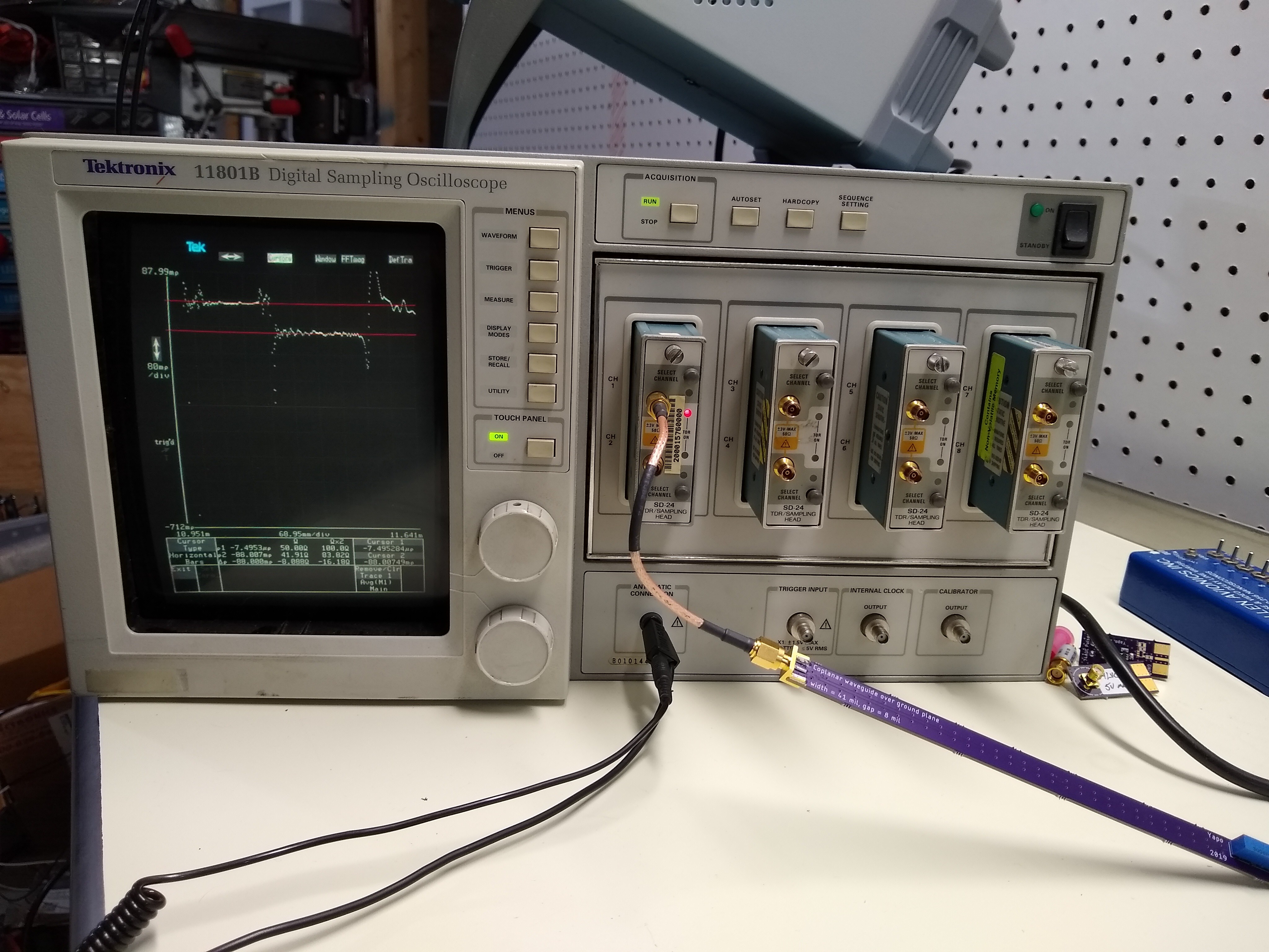
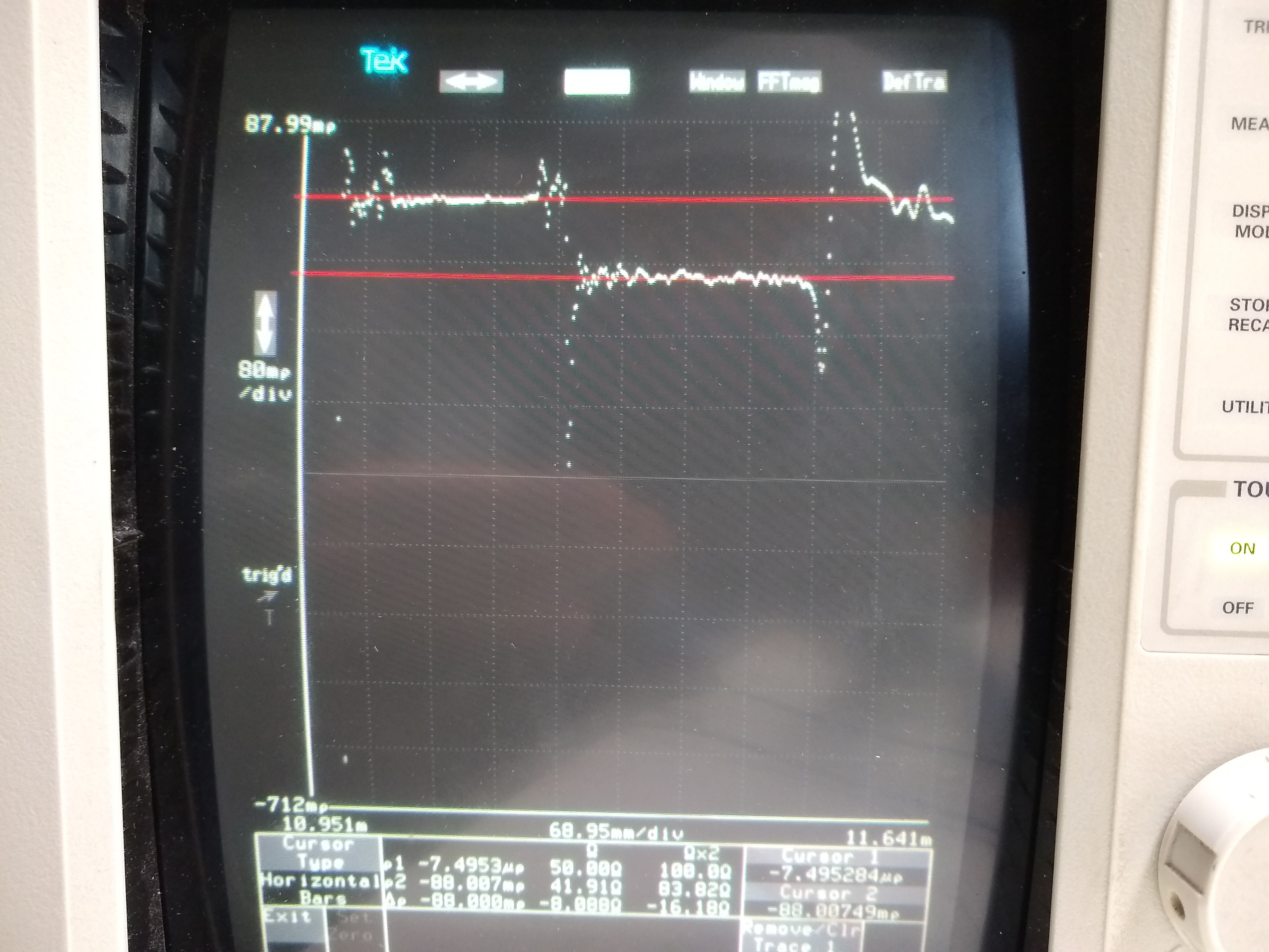
TDR Measurement
I also tried looking into the probe with the TDR capabilities of the scope. In this case, a pulse is send in reverse down the probe coax, and any reflection(s) are observed. It's important to note that because these are reflections, the timescale is stretched by 2x.
![]()
![]()
[placeholder for insanely broken editor which deletes style from paragraph tags]
I added both screen shots so you can see that the impedance - note the vertical scale is in Ohms - does eventually rise to 500 Ohms, the level of the top cursor. The bottom cursor is 50 Ohms.
The 13 mm resistor length is about 43 ps electrically, assuming an air dielectric. So, the round-trip reflection of the end of the probe tip should be around 86 ps after the end of the coax. This is roughly at the first little bump in the response, so that kinda makes sense. I'm not sure what to make of this data, really. Can anyone lend a clue?
Shielding
I noticed that adding capacitance with the trusty finger probe knocked down the inductive bump in the response, so I decided to try adding shielding to the probe. First, I wrapped both conductors in couple of layers of kapton tape.
![]()
Then added a layer of copper foil:
![]()
At this point, it's not really a usable probe anymore, just an experiment. The initial inductive bump is knocked down, now only a 25% overshoot for less than 100 ps or so. This wouldn't be a terrible probe, really, if it were in any way usable physically.
![]()
Add Capacitor
So, what about compensating the probe with a lumped capacitor? I held a few caps on the probe to see the effect, and finally decided on a 1 pF ceramic disc. An SMD cap would be a better choice, but this was handy, so I used it.
![]()
With this cap in place, the initial rise time is a little longer, but the overshoot is down to around 50%.
I would say that the response is acceptably settled by 400 ps, so the probe is probably OK out to maybe 900 MHz.
![]()
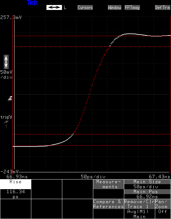
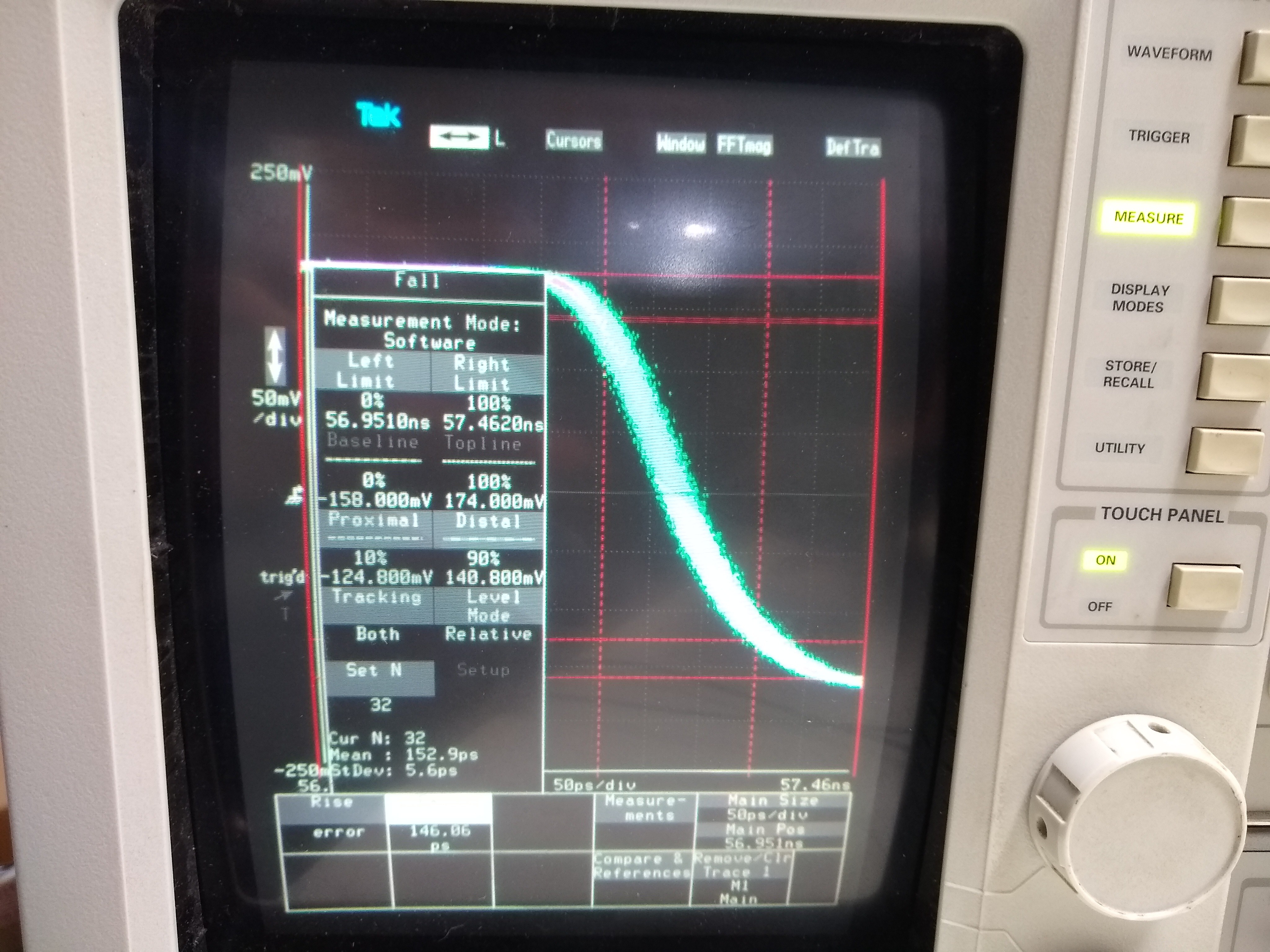
122 ps Step
I dragged out one of my pulsers to test this probe with a more realistic waveform - who's really going to use such a contraption with 20-something ps edges, anyway? This pulser, using an ADCMP606 CML comparator, creates a nice 122-ps step. The left image shows the step directly input to the scope; the right image is measured through the resistive probe:
![]()
![]()
[placeholder for broken editor]
The overshoot here takes around 400 ps to calm down. I would say the probe is not suited for edges this fast.
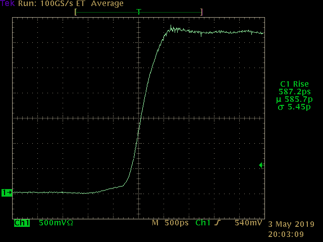
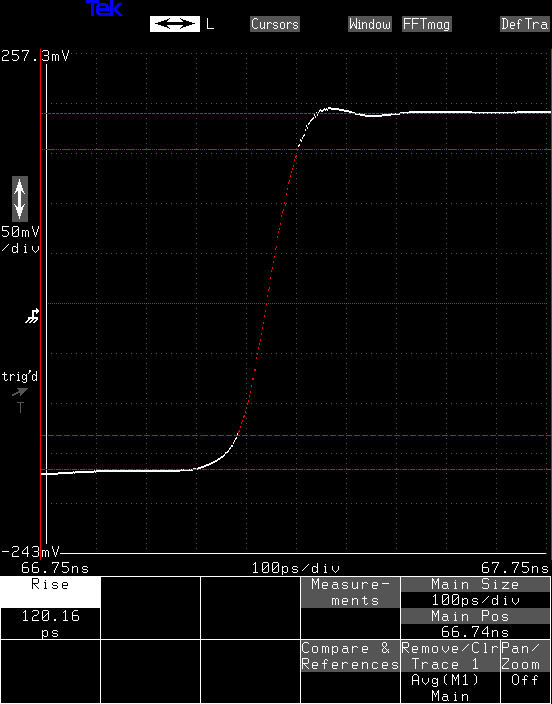
554 ps Edge
This is an edge from a 74LVC1G04 gate, with a 554 ps rise time (left), and the probe output (right). The rise time measured with the probe is 586 ps. It's also on a 1 GHz scope this time, so both these numbers are a little off; the rise time of the scope itself is in the 300 ps range.
![]()
![]()
[editor placeholder]
This time, the overshoot isn't noticeable. This is consistent with the observation that the overshoot takes 400 ps to settle.
Conclusion
This probe looks good for edges of around 400 ps or more. That's equivalent to around 875 MHz.
I'm guessing you can push it above 1 GHz just by trimming the leads a bit. You can probably trim at least 5 mm off the leads.
-
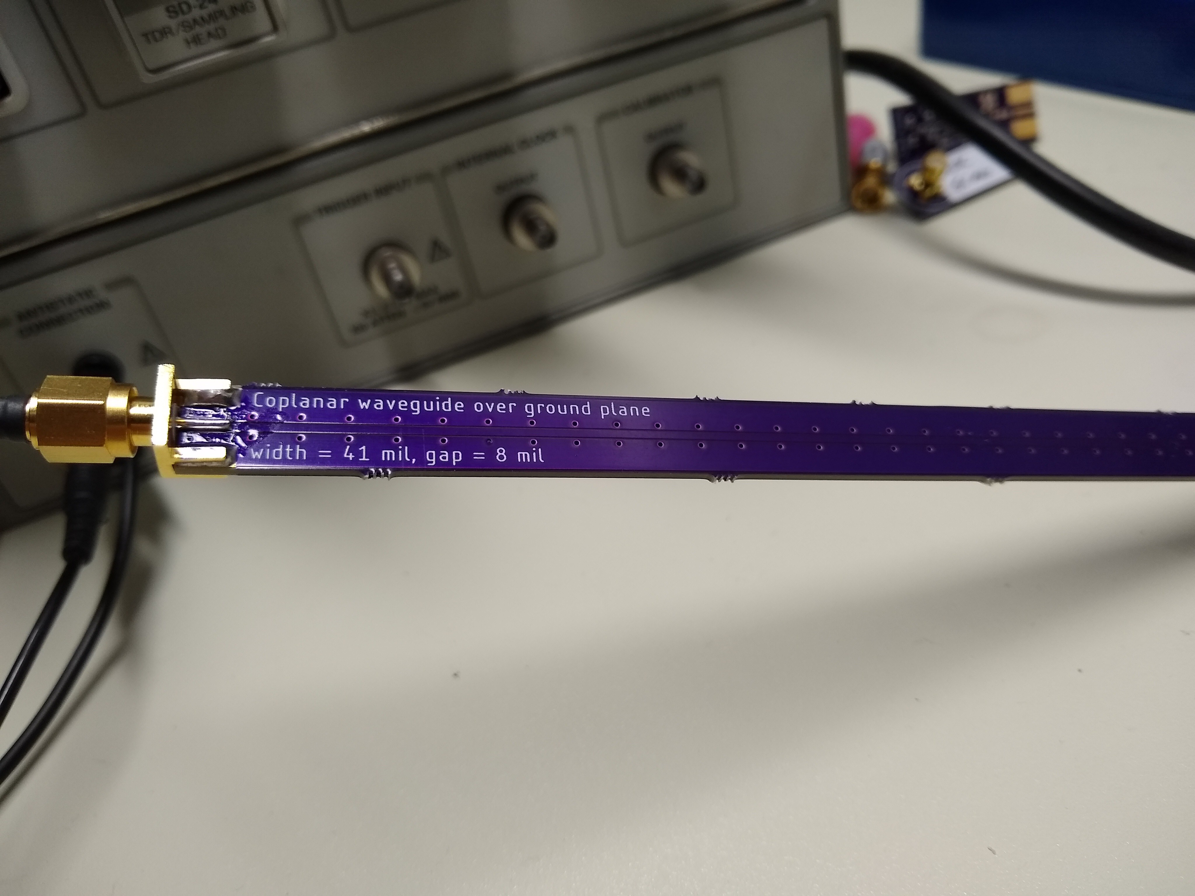
PCB Trace Impedance Revisited
05/02/2019 at 15:51 • 0 commentsI had some 2-layer boards made to test assumptions about coplanar-waveguide (CPWG) over ground plane traces. I also used this test to explore issues with SMA-connector footprints.
![]()
I understand that this is just normal "random" FR-4 substrate, whose properties can vary widely, but the CPWG structure doesn't seem extremely sensitive to dielectric constant changes in the substrate. It does appear to be sensitive to the soldermask, though, for reasons I'll get into below.
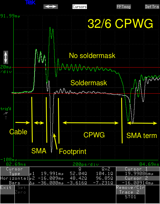
32/6 CPWG
I tested two CPWG geometries, both of which calculate out to 50-Ohms on (most) trace impedance calculators. The first, which seems relatively popular, has a 32-mil trace with 6-mil gaps to the top ground plane on either side; there's a solid ground plane on the bottom of the board. I also tested two different SMA footprints on these traces. One uses the same old footprint I had been using, which has a capacitive impedance bump due to the thick center pin of the SMA connector, while the other has some of the top ground plane cut away -- with a knife -- to compensate.
You can see a whole bunch of stuff in the annotated TDR trace below. Starting from the left, we first see the RG-316 cable, which measures out as 48.42 ohms (it's spec'd 50 +/- 2). Next, there's an inductive (positive) bump due to the mated SMA connectors. After that, there's the PCB footprint for the connector. In my old footprint, you can see a large capacitive (negative-going) bump, while in the cut-away version, you can see I removed too much copper. Back to work on that one.
The central flat portions are the traces themselves. Without soldermask, the trace measures 52.0 Ohms, while adding the mask brings it down to 48.4 Ohms. Both traces would have more than 34 dB return loss, and are actually within the tolerance for common "50-Ohm" cables, so they're probably equally fine for all but the most critical uses.
![]()
It's very interesting that the soldermask makes a difference of 3.6 Ohms in this case, though. I think what's happening is that because the ground plane is so far away in the 2-layer board compared to the side gaps (60 mils vs 6 mils), a lot of the energy is carried in the gaps rather than the substrate. So, adding soldermask with a dielectric constant of around 3 into the gap makes a big difference. I would expect the effect to be smaller where the gap-to-thickness ratio was smaller, like in 4-layer boards, or traces with wider gaps.
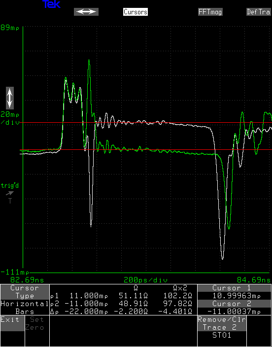
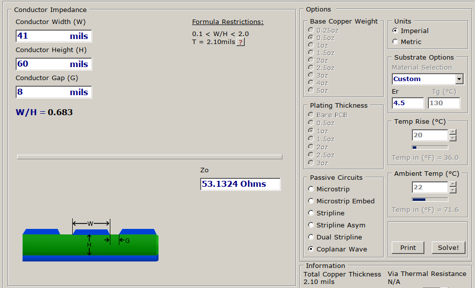
41/8 CPWG
Here's another CPWG structure that calculators put at 50 Ohms, this one with wider gaps.
![]()
Again, the bottom trace is without soldermask and the top trace has it applied - ignore the trace colors, they are opposite from the plot above. As expected, the wider gap means that the soldermask has less influence on the characteristic impedance, in this case 2.2 Ohms vs the 3.6 Ohms for the 32/6 structure. Again, both these traces are perfectly good "50 Ohm" equivalents, so it really shouldn't make much difference. Unless your design rules don't support 6-mil gaps, there's probably no reason to use a 41/8 trace, unless you need a 41-mil wide solder pad for some component.
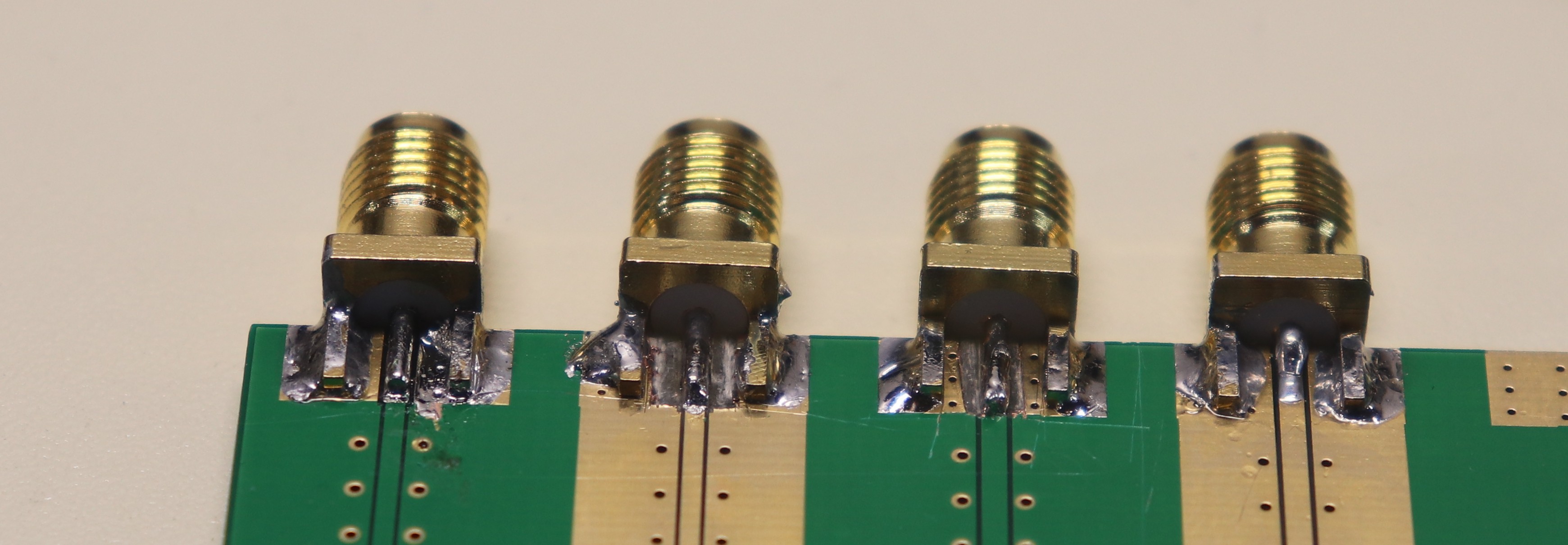
SMA Footprints
One of the places you might need a 41-mil solder pad is on edge-launch connectors. Some of them have wide pins that need a pad wider than 32 mils. The problem, though, is that the round pin itself introduces some capacitance. This can be seen as a dip in the TDR trace. For two of these tests (the outer SMA jacks on the left and right sides in the image below), I used my "standard" SMA footprint, which has a 41-mil wide trace for soldering the pin, and 8-mil wide gaps. Without the pin there, this is just the 41/8 CPWG tested above - you can see this on the rightmost jack, where the trace seems to got right to the board edge.
For the center two, I tried cutting away some of the ground plane on either side to widen the gaps. You can see in the traces that this has the intended effect - the capacitive bump was removed, and was replaced with a slight inductive bump. On the second try, I removed less copper, but it was still a little too much. In any case, this shows the way forward - I need to re-design the footprint with wider gaps at the sides. I don't know exactly how much, but I can guess and try again.
Or maybe get an openEMS simulation going.
![]()
Why not just make it perfect?
With the variability of FR-4 on 2-layer non-impedance-controlled boards, it would seem that chasing a better impedance match would be a waste of time, but at the moment I have nothing better to do, so I'll give it a shot. I'd like to get a good footprint designed, and a "standard" CPWG geometry, and then just be able to use them going forward.
Don't Do This
You might notice that I removed the soldermask from the SMA connector footprint. Never do this - it it incredibly easy to bridge the gap with solder, then you have to spend a long time cleaning it up. For this side of the PCB, I got smart and used some kapton tape to mask the traces, but the other side of the PCB is a disaster. You can see it in the header image at the top of this log.
-
Missed it by 12 picoseconds
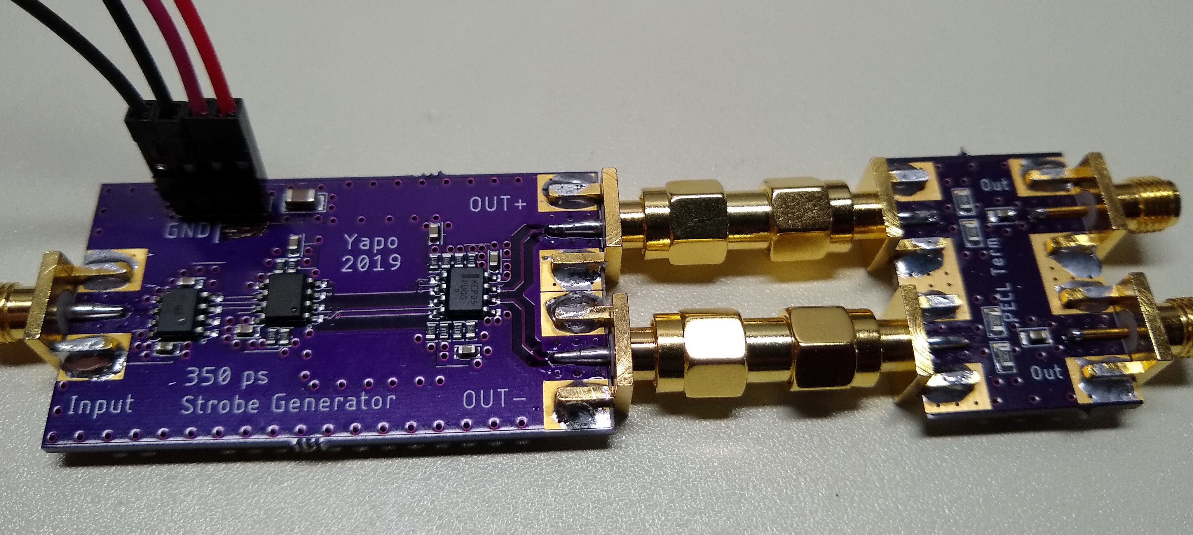
04/21/2019 at 16:17 • 5 commentsI designed this circuit two months ago, but had no way to test it until recently. The goal was to create a 350 ps differential strobe pulse for driving a diode sampling gate (a 1 GHz bandwidth sampler). I populated the board late last night, and it only took an hour this morning to figure out one of the ICs was backwards :-)
![]()
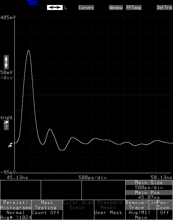
The board on the right is a termination so that I can look at the output with a 50-Ohm oscilloscope input. Shorting the PECL outputs directly into 50 Ohms tends to burn them out :-) Even with the seemingly short interconnects here, this still generates some reflections, which you can see in the second trace below. Those SMA adapters aren't short from the circuit's point of view.
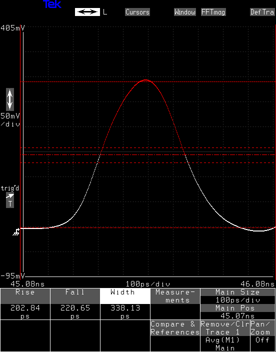
The Pulse
So, here's the output: a 338 ps pulse. The silkscreen on the PCB says 350, so I'm only off by 12 ps, or 3.5%. I'm pretty happy with the result. The amplitude isn't calibrated correctly here, since the output is attenuated by the terminator and the trigger pickoff delay line - did I do a log about that yet? Anyway, the outputs are differential, so there's also a negative-going pulse similar to this one.
![]()
On a larger timescale, you can see the reflections caused by the poor termination. In the actual system, these lines would be properly terminated at the receiver, probably eliminating these bumps. In any case, these aren't likely to be large enough to bias the sampling diodes into conduction, so they don't matter, anyway.
![]()
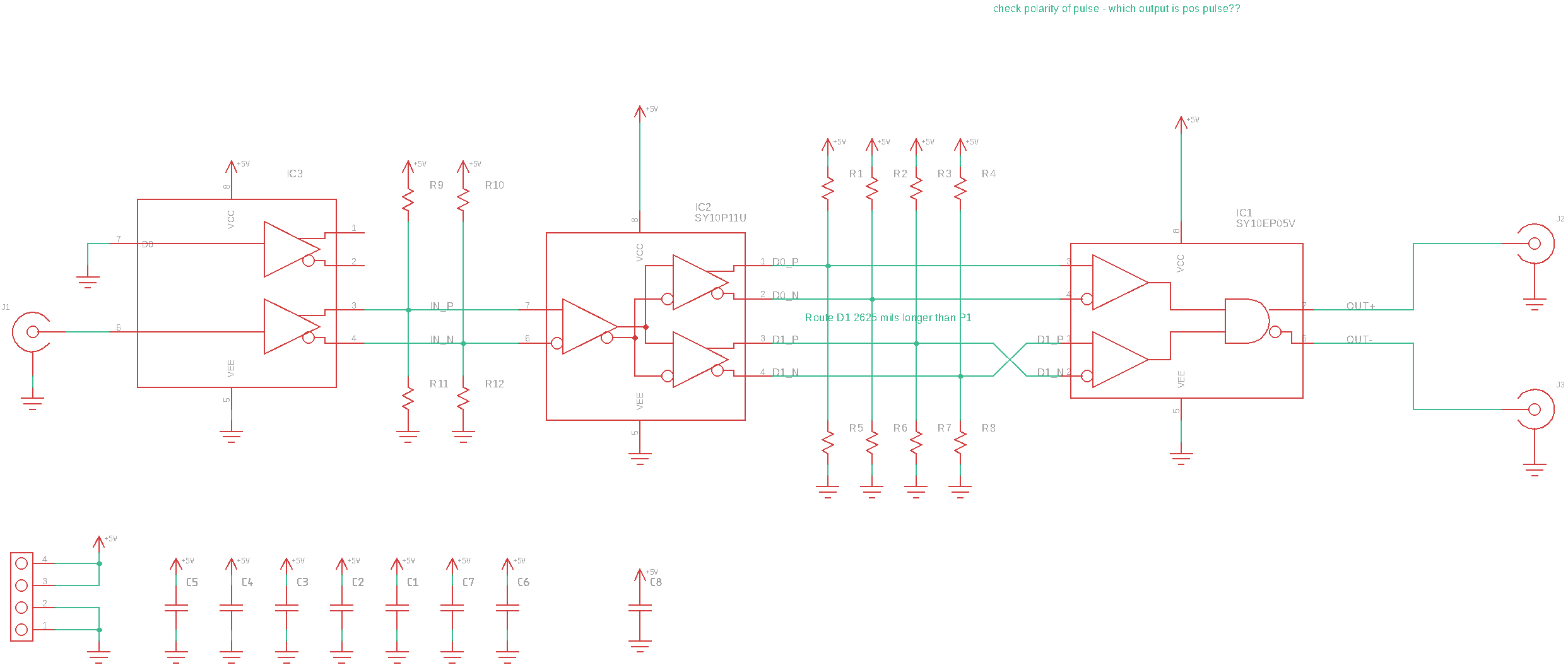
The Circuit
The uses the difference in length between two differential pairs to determine the output pulse width. An SY100EPT22 translator converts the LVCMOS input into 3.3V LVPECL outputs. This output is duplicated by an SY100EP1U 2:1 fan-out buffer. The 20 ps maximum output skew on this part could account for my 12 ps error. The two outputs then feed into an MC100EP05 AND/NAND gate, but one of them is delayed by going through longer traces on the PCB. On each incoming pulse edge, the output goes high briefly, until the delayed signal comes along to turn it back off again.
![]()
All of the pullups are 127 Ohms, and the pulldowns 82.5 Ohms, which is the Thevenin equivalent of terminating the lines in 50 Ohms to Vcc-2 V (for a 3.3V supply). The resistors dissipate more heat than you might expect - unless you've done the math, that is.
The output driver has a typical rise/fall time of 220 ps, which ultimately limits the minimum pulse width. You can try to make it shorter than this, but then the amplitude of the pulse starts to drop.
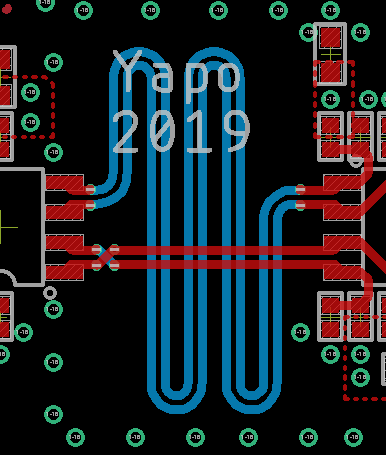
The Delay Lines
Here you can see the lines that determine the pulse width. The red traces are on the top of the 4-layer PCB, while the blue ones are on the bottom.
![]()
With a dielectric constant of 3.66, the OSH Park 4-layer process should have a velocity factor of 0.523, so signals should travel at 1.568e8 m/s. This is equivalent to a delay of 162 ps/inch. The shorter red pair is 492 mils long, while the longer blue one is 2643 mils long, for a difference of 2151 mils. This equals a delay of 348 ps, so hey, I'm only really 10 ps off!
So What?
The original plan was to use a pulse generator like this for a sampling head strobe. I'll probably still build one using this design, but have shifted my attention to pulse generators using inexpensive laser diode drivers instead. The PECL gates on this PCB are expensive, power hungry, and ultimately too slow for where I want to go. As a demonstration, it's not bad, and it's probably still worth developing into a full sampling head just for the experience, but there's no future in it.
On the other hand, this board validated a bunch of assumptions and techniques that I'll need later.
-
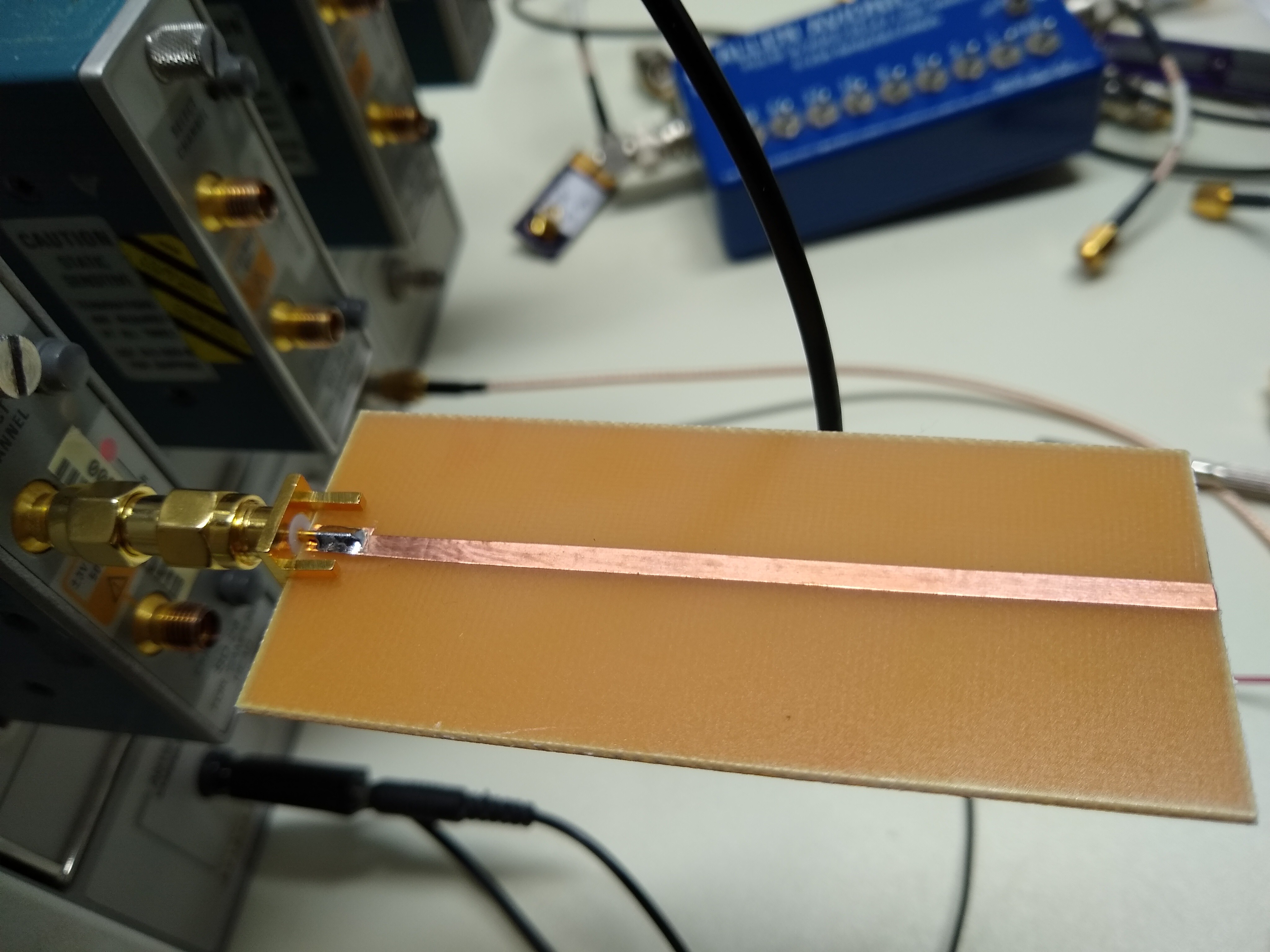
A quick one: copper-tape prototypes
04/19/2019 at 15:04 • 8 commentsA long time ago, I read somewhere about using 0.125" (~3mm) copper foil tape to create 50-Ohm traces on the back of single-sided copper clad board for quick RF prototypes. This width is very close to the usual 110-mil trace width you'd use on a PCB. Yesterday, I decided to try it out.
![]()
To run a trace, you just stick the tape to the PCB. The bottom of the PCB is un-etched solid copper which acts as the ground plane. I've done circuit prototypes this way before, but never really investigated the technique.
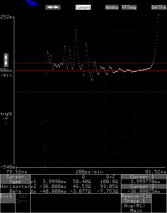
With the full 125-mil width, the impedance is a little low, reading around 46.5 Ohms. Don't worry if you find it difficult to interpret the trace. I found that I can locate what's what on the screen by touching the PCB trace with the tip of a screwdriver; the added capacitance shows up as a bump in the response. 46.5 ohms isn't bad - that's under 1.08 VSWR, and 29 dB return loss. You can also see how my lousy cheap M/M SMA adapter and board launch cause all sorts of bumps. Quality microwave connectors are expensive for a reason.
![]()
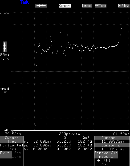
I tried cutting the trace down slightly (the image above is of the trimmed foil - you can see a little notch right after the BNC connector. I removed too much foil, and ended up at 51.2 Ohms. This is a little better at 1.03 VSWR and around 38 dB return loss. Whether this extra precision is worth the effort depends on what you're doing.
![]()
There's a lot more that would be interesting to look at - like loss, for instance - but being able to whip up some prototypes quickly without etching, milling, or waiting for PCB fab services sounds pretty appealing.
The problem, of course, is that this microstrip trace is really big. I wonder if I can find some thin single-sided copper clad that would bring down the trace width?
-
Back to the beginning: ADCMP606 w/ 120 ps edges
04/17/2019 at 02:15 • 5 commentsI started this project with a pulse generator based on a ADCMP606 CML-output comparator. It was faster than my scope at the time, so all I could really say was that the rise-time was less than 350 ps or so. Last night, I found some quality time with the new scope, and measured the rise time of that circuit at less than 120 ps.
![]()
At a longer timescale, the step looks pretty good, with minimal overshoot. It's a handsome pulse, attesting to the robustness of the comparator in the face of my inept board design :-) This comparator has a datasheet rise time of 160 ps, which implies typical Analog Devices understatement/over-performance.![]()
Overall, for a $6 (single-quantity) part, it's not bad at all. I think I'm going to make another revision of this board and release it. With a 120 ps rise-time, it's certainly good enough for testing oscilloscopes up to around 2 GHz.
-
Validating PCB Transmission Lines
04/12/2019 at 23:42 • 24 commentsSo, I finally found some time to measure the impedance of a test PCB with the new TDR scope. I had made the PCB up a while a go to start validating the proper dimensions for controlled-impedance structures on the OSH Park board stackups, but didn't really have the equipment to measure it accurately until now.
![]()
The TDR mode on the scope has direct readout in Ohms (vertical) and either time or length - if you know the velocity factor - on the horizontal. Of course, if you measure the time with the scope, and the physical length with a ruler, you can calculate the velocity factor - which will be my next step.
The measurement results in 50.0 Ohms for the coax jumper, then 41.91 ohms for the PCB trace. It also shows that my PCB footprint for the SMA connector has a nasty reflection. I need to fix that.
![]()
I used an on-line calculator to come up with the dimensions for this coplanar waveguide over ground plane. It gave me a 14 mil trace width and 8 mil spacing for OSH Park's 2-layer stackup. I realize that this is just plain "random" FR4, but I wanted to start with something inexpensive. I also realize that the dielectric will probably change from batch to batch, so I'm not going to chase this one too far. I'm much more interested in the 4-layer stackup on FR408 dielectric.
![]()
The thing that bothers me, though, is that Saturn PCB toolkit, for example, says this line should have a 53.2 Ohm impedance.
![]()
Calculators are stupid. I need to learn how to use a real electromagnetic simulation program.
Maybe I was right?
I did try to measure this with my own TDR before, but I didn't trust the results. I'll have to go back to my notes and see what I came up with before. I could have dismissed my results if I saw this large discrepancy before.
-
Good news and bad news
04/11/2019 at 01:00 • 0 commentsThe good news is that I can finally measure the fast and/or short pulses I've been working to make. The bad news is that they're not what they should be. The laser-driver pulse generator from a few logs ago measures out around 150 ps fall time. It should be much less than this - less than 40 ps, ideally. I haven't managed to measure the rise time yet.
![]()
There could be any number of reasons for this, including my use of inexpensive - and physically large - passive components instead of high-frequency types. My PCB design probably doesn't help. There's a list of rise-times of various connectors and cables in the "black magic" book - I should add up the contributions from all the junk I have in the signal path, too.
There is also a lot of jitter - I'm not actually sure I'm seeing the edge associated with the trigger here. If it were some later edge, that might explain much of the jitter.
It's a little disappointing that the thing didn't "just work," but still exciting that I can see what's going on and iterate until it works.
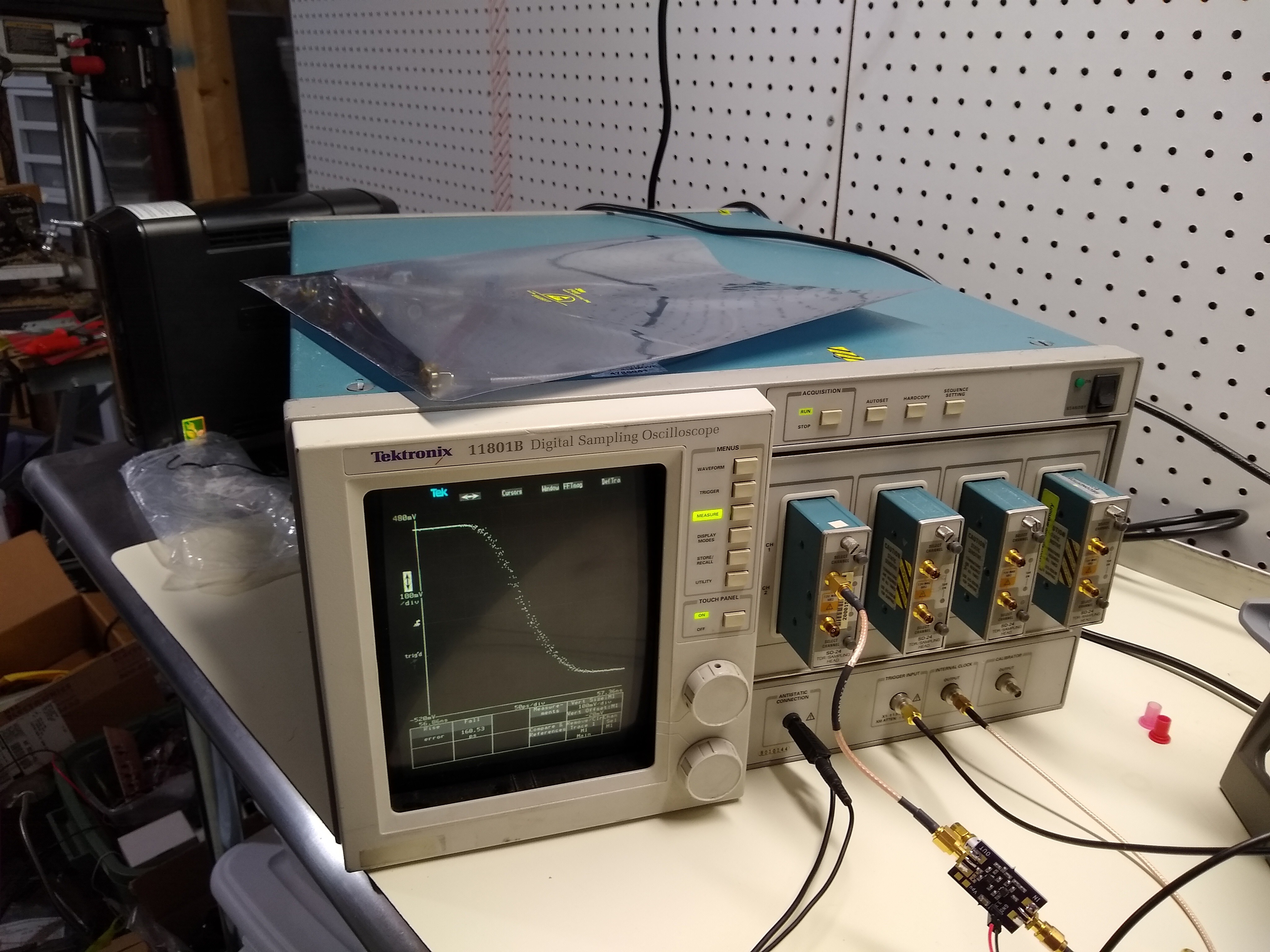
The machine behind the new measurements is this Tektronix 11801B with four SD-24 sampling heads. It arrived today from ebay, and I just finished a first test - all eight 20 GHz channels seem to work fine. The thing is a 60-pound monster, and I'm going to need to find something to put it on, because it takes up half my bench.
![]()
I was in college around 1990 when this was new. It sold for around the same price as my entire education. We are so amazingly lucky to live in the time of ebay.
-
A diode bridge for sampling
04/04/2019 at 02:33 • 0 commentsI found a very nice diode array which seems perfectly suited for a fast sampling oscilloscope front-end. The Skyworks SMS3923-081LF has four fast Schottky diodes in a dual series pair arrangement. It comes in a tiny 6-lead SC-88 case, and the datasheet has a model for the package parasitics as well as SPICE parameters. I made an LTspice component from it.
![]()
At first I forgot to add the "p" to the CJO parameter, making it 0.9 Farads instead of pico-farads. This did not simulate well.
The only thing I don't particularly like about these diodes is the diffusion transit time (TT SPICE parameter) of 80 ps. I wish it were smaller, but the truth is that I'm not going to get strobe pulses anywhere near that short, at least in the near future.
Other than that, it looks like a winner.
I'm still playing with some simulations of this part. I'll update the log with results soon.
-
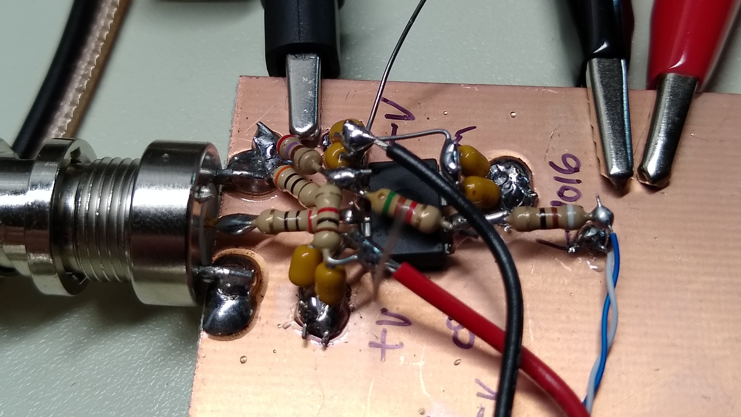
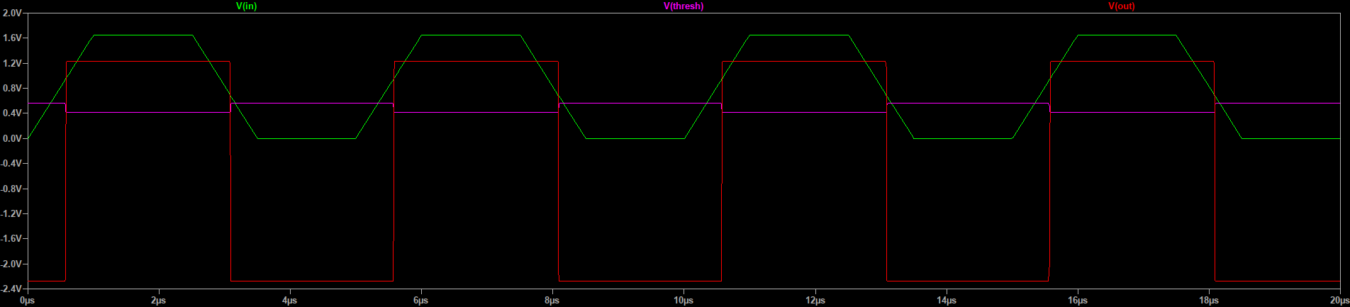
Comparator Voltage Translator
04/01/2019 at 12:55 • 0 commentsI'm documenting this here so next time I do it, I can just look this up. I needed a decently fast level translator from LVCMOS (3.3V supply) to CMOS logic run from a +/-2.5 V split supply. Running logic from a split supply is not something you see very often, so there aren't commercial translators which will do the job.
![]()
I had a small bag of LT1016 comparators, so I decided to go with that. This comparator was very fast for its day, and it will do for now, although all these years later, there are certainly faster options available. In any case, proper layout is essential with fast comparators, and a healthy dose of positive feedback (hysteresis) keeps things stable.
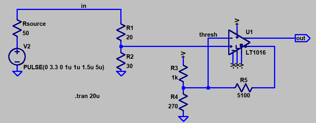
I didn't want to jam noise back into the input in this case, as you would usually do with a hysteresis arrangement from a non-inverting comparator output. Instead, since the comparator has true and inverted outputs, you can take feedback from the inverting output to the inverting input. This is positive feedback, and makes for some nice hysteresis, which also doesn't depend on the impedance of the input source. In any case, the circuit looks like this:
![]()
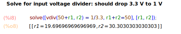
I used wxMaxima to calculate the resistor values. First, the input divider, consisting of R1 and R2. I want this to terminate the input connector in 50 Ohms and also divide the incoming 3.3 V logic signal to a 1 V level. I chose 1 V because the common-mode range of the LT1016 only extends to around 1 V in this circuit (V+ - 1.5 V).
![]()
Easy enough. 20 and 30 Ohms are standard 5% values, of which I have a lifetime's supply in 1/4 W through-hole.
Hysteresis Calculations
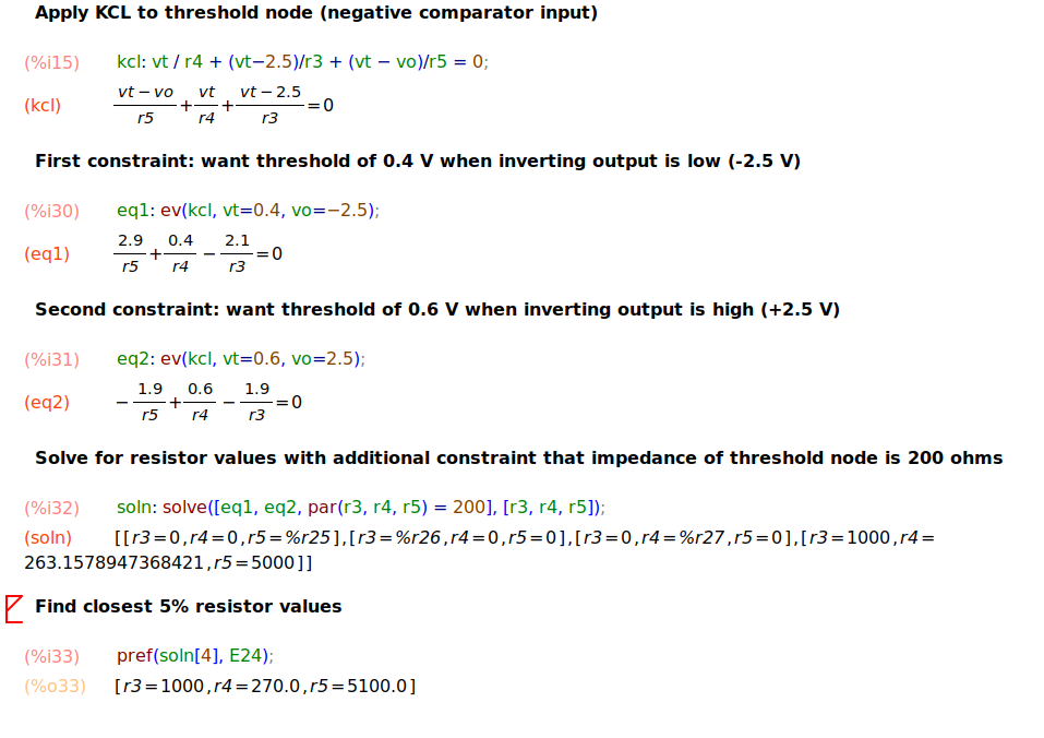
Solving for R3-R5, which determine the hysteresis, is a little more involved. I wanted the thresholds at 0.4 V and 0.6V, for 200 mV of hysteresis. I also wanted the impedance into the inverting input of the comparator to be relatively low, somewhat arbitrarily choosing 200 Ohms.
The approach is to apply Kirchhoff's Current Law (KCL) to the feedback node and create an equation for each of the threshold states. An additional equation sets the impedance of the node to 200 Ohms.
![]()
Simulation and Test
Since the LT1016 is a Linear Technology device, it has a model in LTspice. Simulation revealed something I hadn't considered: the outputs are not rail-to-rail. I may have CMOS on the brain. Instead of providing 2.5 V when high, the outputs are closer to 1.2 V.
![]()
The hysteresis levels in simulation are 420 mV and 558 mV. On the bench, the circuit worked fine with no problems observed. I don't have oscilloscope shots from the bench testing, but they were rather boring anyway.
The circuit seemed to give nice, square outputs up to 20 MHz, then everything kind of started looking linear-ish. I've read that the gain drops off precipitously in these devices around this point, so it's not really surprising. When I get some more time, I'll go back and measure the performance up to 120 MHz or so, which is the limit of my current DDS generator.
If I make this particular circuit again, I might use slightly different resistors to compensate for the lower output values. Using the LTspice simulations shows that the inverting output swings from -2.24 V to +1.22 V. Re-running the maxima calculations gives { R3 = 910, R4 = 270, R5 = 3600 }. Simulation with the new values shows thresholds of 418 mV and 606 mV. These aren't really that different from the ones I originally chose, so maybe it doesn't make much difference.
In any case, I have a decent translator to connect things to logic driven from split supplies now. The output isn't fully rail-to-rail, but the +1.2 V high-level voltage is enough to meet the CMOS high-level input minimum of 1.0 V for the 74LVC gates I'll be driving with it. a more modern comparator might be even better.
The Rise and Fall of Pulses
A project in which I try to go faster and faster