Close
0%
0%

Multiplexed ESP8266 nixie clock project

A design for an ESP8266 based Nixie Tube Clock, suitable for home-made PCB construction

Similar projects worth following
1.7k views
A design for an ESP8266 based Nixie Tube Clock, suitable for home-made PCB construction

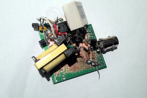
I've made a number of Nixie and VFD tube clocks over the past few years, often using professionally manufactured PCBs I designed.


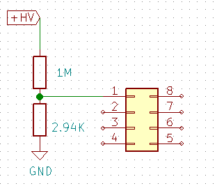
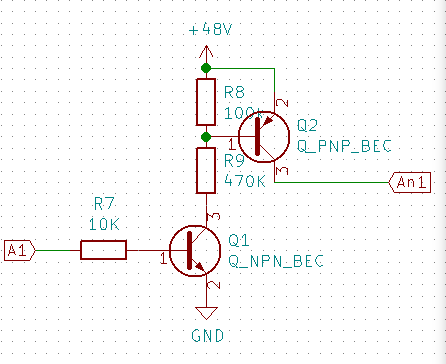
For 2019, I thought I'd go back to basics, and make a PCB design I could fab at home, using easy to source components (such as high voltage NPN and PNP transistors, and shift registers).

That limits me to a single sided board, which I can etch at home using photolithography.

  • Nixies, current, pulses, strike voltages

    David Pye02/02/2019 at 23:17 3 comments

    I have been running a few experiments with my IN-12 nixies this evening, to try and decide how best to set pulse voltage/current.


    The IN12 Soviet data sheets do not specify any details for pulse operation, but the side-view IN14 nixies do.  They specify similar direct drive parameters, so I have extrapolated these to pulse operation.

    I am aiming for a strike voltage of 190V, and pulse current of 8-13mA.  However, there's no mention of how to calculate an anode resistor here.

    So I have decided to do it experimentally (and using some helpful advice from the neo-nixie google group!)

    In order to measure pulse current, you need an oscilloscope, and measure the voltage drop across the anode resistor during the pulse. From this, and the known value of the anode resistor, you can work out what the pulse current through the resistor (which also flows through the nixie) will be.

    From my Rigol scope, using a 3k9 anode resistor, I got this:

    Using a strike voltage of 200V, and that value of anode resistor, the voltage drop across the resistor during the pulse is ~43V.  With another nixie tube, it was 50V.

    So, using Ohms law, a current of between 11mA and 12.8mA is flowing, so this is about right.  This means the sustained voltage across the tube (once it has struck) is around 150V.

    So, here is a scope plot of the voltage across the tube during the pulse (note the Y axis scales are different!)

    So, you can see that at the start of the pulse, the full 200V appears across the Nixie, it strikes, and pulls the voltage down to the sustain value (which, with the anode resistor dropping 50V), is 150V as expected.

    For interest, i decided to zoom in on the first part of the pulse, to better visualise what happens when the nixie strikes:

    So, you can see for about 18microseconds, the nixie doesn't conduct, then over the next 12microseconds, it starts to ionise and conduct, and by 30microseconds after the start of the pulse, it reaches steady state.

    So, I'm fairly happy that my anode resistor value of 3k9 is about right here, for pulsed operation.


    I intend to produce some graphs showing current in pulsed mode for both IN12s and IN14s to aid other experimenters...!

    David

  • Modifying the high voltage DC-DC converter

    David Pye01/25/2019 at 18:59 1 comment

    So, for the multiplexed clock, I need an anode voltage of 190V.

    However, the DC-DC converter board I have is fixed voltage,  170V.   ( from https://www.ebay.co.uk/itm/DC-5V-12V-170V-DC-High-Voltage-NIXIE-Power-Supply-Module-PSU-NIXIE-TUBE-ERA-/332647890313)

    I wonder how fixed it really is....

    Close-up, front and back, it looks like this:

    Note that somebody has kindly ground off the part number etc from the main IC, so we have no idea what it is (presumably to make it harder for people to duplicate), but it also makes it hard for us to work out how to adjust it.

    Most DC-DC converters use an arrangement a bit like this to set/maintain the voltage:

    Where the output voltage is split via a potential divider and fed back into the chip, so it can adjust/stabilise it.

    So, we need to find something on our schematic that looks a bit like that kind of layout.

    Those two resistors  (circled) form a potential divider which is stretched across the HV output, to ground, and the middle of them is connected to Pin 1 of the mystery IC.

    So, I decided to try experimenting with changing the value of the 2.94k resistor (labelled 2941), as I suspected it set the HV output.

    That gave me the following outputs:

    • Resistor value: 2.94k   - 170V output
    • Resistor value: 2.36k : 215V output
    • Resistor value: 2.59K: 197V output
    • Resistor value: 2.65K: 192V output

    From those, I selected 2.67KOhm as the new resistor value as it's a standard value.

    This will give me 192V which is close enough to the 192V I need for multiplexing according to the datasheet, and below the 'absolute maximum' rating of 200V of the tubes.

    Of course, I don't actually know the ratings of the components within this DC-DC converter, but it seems to still function OK, and not get too warm.  I'll have to see what its' longterm longevity is like....!

  • Basic design of the clock

    David Pye01/20/2019 at 22:32 0 comments

    For this clock build, I've selected the following components:

    • An ESP8266 based microcontroller board.  I've picked the Wemos D1 mini because it's cheapish, I've used it before, and it's easy  to program via USB.  It's also wifi capable, so you can send it messages etc and make it display something other than the time if you like.
    • An eBay sourced DS3232 RTC with backup battery to provide the time for the clock.
    • 5mm neopixel LEDs to backlight the tubes for a nice visual effect.
    • IN-12 nixie tubes because they're cheap, but you can use most types with a few tweaks.
    • An ebay sourced TINY 170V DC-DC converter that takes 5V in, and outputs 170V to drive the tubes.
    • Discrete NPN/PNP transistor drive using MPSA42/MPSA92 transistor pairs in SOT-23 form factor.
    • Four PCB mounted switches for setting time etc.
    • An LDR to allow the clock to dim in response to changes in ambient light.
    • 74HC595 surface mount shift registersx2 to provide the right number of IO lines.

  • Design of the high voltage driver circuitry

    David Pye01/20/2019 at 22:25 1 comment

    This clock is designed to multiplex the nixie tubes.

    This means that only one tube is illuminated at any one time, and the code turns each tube on and off quickly enough that your eyes see them all as being on simultaneously.

    A nixie tube has one anode, and a number of cathodes.  Most numerical display tubes have 10 cathodes (digits 0-9) although some have as many as 12 (two decimal point cathodes - leading and trailing).

    For direct drive designs the number of output lines from the microcontroller to drive the displays are 10 * number of tubes.

    For multiplexed designs, the number of output lines required for switching is 10 + the number of tubes.  So, for a 6 tube clock, a total of 16 output lines are required.  Conveniently a pair of 74HC595 shift registers will provide 16 bits of output.

    Advantage: Less circuitry  + IO required, easier wiring

    DIsadvantage: More software complexity and timing.   Less bright for given current, so much higher current pulses are required to achieve the same brightness as a direct drive design, which may wear out the tubes more quickly (may - there are many different viewpoints on this!)

    Most multiplex designs use the following basic design:

    • Wire the same cathodes on each tube together.  So, for example, each tube's 0 digit cathodes are connected together, each tube's 1 digit cathodes are connected together etc.
    • To illuminate a specific tube, that tube's anode is driven HIGH (ie to the HV supply ~170V) to select it.  
    • The desired cathode is pulled to GND.
    • A short blanking interval occurs where no anodes are pulled high, and the process then repeats for the remaining tubes.
    • Cycle repeats


    Microcontroller pins can't drive high voltage directly, so transistors are often used.   Controlling the cathodes to pull them to GND Is easy, and can be done with a high-voltage capable NPN transistor, such as an MPSA42, like this:

    When address line C10 is pulled HIGH, the transistor conducts, and Cat10 here is connected to ground, illuminating that segment.

    However, pulling an anode 'HIGH' to select a tube is harder, as this requires level switching.  This design uses the following schematic: (+48V is actually +HV @ 170volts), and A1 is the address line.  AN1 is the wired to the anode of Nixie 1.  Q1 is an MPSA42, and Q2 is the PNP version (MPSA92).

    So, when the address line A1 goes HIGH, the transistors switch, and 170V is applied to the tube's anode, thus selecting it.

    So, the HV drive circuitry for this design consists of:

    10 x the cathode drive circuitry

    6 x the anode drive circuitry

    (Actually, there is a spare cathode drive circuit, which you can use to drive some neon indicators for decimal points etc if you like!)

View all 4 project logs

Enjoy this project?

Share

Discussions

Similar Projects

Does this project spark your interest?

Become a member to follow this project and never miss any updates