Bil Herd
(The original post of this can be seen on Hackaday.com)
Designing circuit boards for high speed applications requires special considerations. This you already know, but what exactly do you need to do differently from common board layout? Building on where I left off discussing impedance in 2 layer Printed Circuit Board (PCB) designs, I wanted to start talking about high speed design techniques as they relate to PCBs. This is the world of multi-layer PCBs and where the impedance of both the Power Delivery Network (PDN) and the integrity of the signals themselves (Signal Integrity or SI) become very important factors.
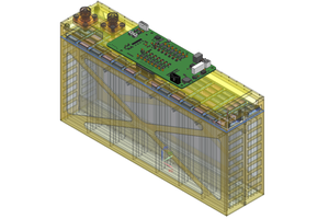
I put together a few board designs to test out different situations that affect high speed signals. You’ve likely heard of vias and traces laid out at right angles having an impact. But have you considered how the glass fabric weave in the board itself impacts a design? In this video I grabbed some of my fanciest test equipment and put these design assumptions to the test. Have a look and then join me after the break for more details on what went into this!
WHAT I MEAN BY “HIGH SPEED”
The term “high speed design” can mean different things to different people depending on what they are used to working with, but for me it’s where the energy of the rising and falling edges of the signals dominate the behavior compared to the fundamental frequency of the signal itself. In other words a 10Mhz signal that has a 1ns rise time has a bandwidth of roughly 350Mhz as seen by the formula below. Ultimately it’s the energy in the rise/fall time of the signal that affects a lot of the design.
The relationship between the bandwidth and the rise time can be approximated as:

With regard to high speed design rules, my first rule of thumb is to be cautious about rules of thumb. I use rules of thumb as an early estimate that helps me to get an idea of how all of my design rules and goals play together.
As someone who has been doing design since the 1970’s I have seen the evolution of assumptions and design guidelines mature and it’s fair to say that there were a couple of things that we got wrong along the way, some things almost comically wrong. For example, I have heard people say that electrons slam into each other trying to turn corners at high speeds so it’s a bad thing to do, we now don’t think that way.
HIGH SPEED DESIGN ASSUMPTIONS
Some of the principles of high speed design are listed below. I can’t get to all of them in this one post but I dowant to get to all of them in turn.
- At high speeds it’s all about the propagation of the Electro-Magnetic (EM) field, not electrons.
- High speed current follows the path of least impedance on a power or ground plane, not the path of least resistance.
- Due to the geometry of the glass fabric weave used in the construction of the PCB, the impedance of a signal trace may change based upon the orientation and the position in relation to the weave.
- Right angle corners in PCB traces may not be near as detrimental as often assumed.
- In a properly designed multi-layer PCB, the placement of decoupling capacitors near the loads may not be near as critical as is assumed.
- Ferrite beads in line with the various voltage traces may do more harm than good.
- Differential pairs aren’t coupled to each other like we often depict, their return current is through the ground plane, not through the other half of the pair of traces.
- Tightly coupling a differential pair may not have as good of noise rejection as two random paths provided they are the same length.
- Since the current flows on the surface of a conductor (known as skin effect) high speed PCB’s may specify smooth or polished copper traces for the inner layers so that the path is smoother and straighter.
EM FIELDS

At high speeds it’s not so much about the flow of electrons but rather the energy in the Electromagnetic...
Read more »
 Rhys
Rhys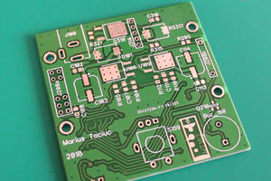
 Marius Taciuc
 Lucy Fauth