 DeepSOIC
What is depletion mode, and why you might want it
Enhancement MOSFET: normally off (the common stuff). Depletion MOSFET: normally on. To switch off an n-channel depletion MOSFET, you should apply negative voltage to gate terminal. That is, it behaves exactly the same as an enhancement n-channel, but it has negative gate threshold voltage. Very similar to a vacuum tube, by the way.
In other words, depletion MOSFET is equivalent to enhancement mosfet with built-in biasing (voltage source in series with gate terminal).
Depletion mosfets are quite rare. Chances of finding one with specs you need are much lower, and depletion mosfets are usually substantially more expensive than enhancement ones.
A JFET is a more common example of a depletion mode FET. But power JFETs are rare beasts, again.
Depletion MOSFETs are not as useful as enhancement ones, but there are a few applications where they are super handy.
One is a voltage follower with zero or negative voltage drop. With just two components (mosfet + potentiometer), one can make a very simple knob power adjustment, that has almost zero dropout at max, and infinite input resistance. It can be used as a quick-n-dirty fan speed adjustment, LED brightness regulator, etc. See this project log for a demo of such regulator.
How to?
Modifying!
To change the MOSFET, all you need is to feed constant current into gate terminal of the MOSFET.
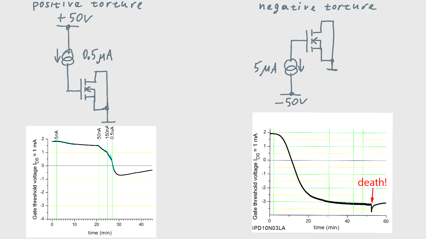
It will take around +40 V / -25 V at gate terminal or the current to start. Because it’s a deliberate violation of absolute maximum ratings of the MOSFET, I call it “torture”.
In both cases, threshold voltage goes down. Positive torture begins to change the transistor immediately, but the negative torture has a kind of lag. This lag seems to be some stray leakage that has to be overcome. The gate voltage rises to about 40 V during that lag. Also, negative torture requires more current, it can reach deeper depletion, and does not reverse direction.
So far, I was not able to make threshold voltage to increase. From that, I think that making depletion mode p-channel mosfets might be impossible (but I haven’t tried yet!).
The indicated torture currents are for Infineon IPD10N03LA mosfet, which is an n-channel enhancement mode MOSFET with on-resistance of 10.4 mΩ, 25 V max drain-source voltage, gate charge of 8.2 nC. No extensive tests on other mosfets were done so far, but I would suggest to scale torture currents in proportion to gate charge of your transistor.
@RoGeorge had successfully modified BUZ11A with positive torture, but didn’t do it in a controlled manner. See his project, #Your MOSFET is not good enough? Then modify it!.
If you successfully modify a MOSFET, let me know! (post a comment). Eventually, I hope to make a table of MOSFETS that can/can’t be modified, and torture parameters required.
Reverting!
It is possible to undo the modification to a large extent, by applying positive voltage to gate. The voltage should be large, but slightly smaller than one required to cause torture leakage current. For IPD10N03LA, +35V seems to be the sweet spot.
Real-time threshold monitoring
Wondering how did I get these plots?
I made two circuits for torturing MOSFETs with real-time control of gate threshold voltage. Both circuits are chopping: the mode of operation is cyclically switched between measuring threshold and torturing.
* “blink torture” circuit – simple, but only for negative torture. Was all-right for initial proof-of-concept.
* “experimentorture” circuit – with precise threshold measurement, supporting both positive and negative torture.
Drawbacks
Sounds too good to be true? Sure, there are some problems with this conversion.
* after torture, the mosfet drifts back substantially. This drift settles out after a day or so, with substantial fraction of modification remaining. Long-term stability of the modification is unknown. However, quite surprisingly, the modification can survive soldering temperatures.
* gate voltage – drain current relationship slope is reduced, thus more change in voltage is required to achieve switching. For details, read project log "Transfer Characteristic".
* after much torture, the MOSFET may become drifty. This presents itself in gate threshold voltage taking a few seconds to settle as I insert a mosfet into measurement rig. This drift is not related to heat, and can be reproduced by unplugging-plugging the mosfet many times in a row.
See also
@RoGeorge’s project #Your MOSFET is not good enough? Then modify it!
Hackaday post about this project
What’s happening
The short and correct answer is – I don’t know! But I do have a few ideas. Let me first explain, how it all started.
...
I've been passively trying to get some depletion mode power mosfets, mainly for making LED torches (flashlights) with adjustable brightness. They are useful because I can make a source follower with zero or negative voltage drop, the output of which can easily go up to the very rail without needing a bootstrap. But I couldn't get them. They are rare and quite expensive, and no one seems to have them in stock. I maybe could have obtained them, but I wasn't desperate enough...
Lately, I was reading a book about semiconductor junctions. Particularly, a section about MOSFETs, and about flash memory. I saw a picture of a flash memory mosfet with no floating gate, and an idea popped up. What if I can get analogous effect on a regular mosfet, that can effectively convert a typical enhancement mode mosfet into a depletion-mode mosfet? Hmm!
Here's the picture from the book:
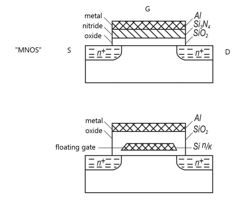
At the bottom, a commonly known flash memory kind of MOSFET is shown. Applying large voltage to gate terminal deposits charge onto floating gate, thanks to tunneling. This charge biases the transistor.
In the upper structure, the (conducting) floating gate is replaced with the interface between insulator materials. The interface has electron states that can be populated and emptied, again thanks to tunneling. The overall principle is essentially the same.
Now, I thought. Hey, SiO2 is likely quite defective in the first place, so maybe it is possible to bias it too?
So the plan was simple. Apply high negative voltage to gate terminal of mosfet, and see if it becomes a depletion mosfet. It worked, so the project was born.
-------------
Now, knowing that applying large positive voltage makes it shift in the same direction, it became clear that in this case, the mechanism is a bit different from what happens in flash memory.
Because I could only achieve gate threshold voltage to decrease, I can conclude that only positive charge can be deposited in SiO2. The picture below is how it looks on band diagram.
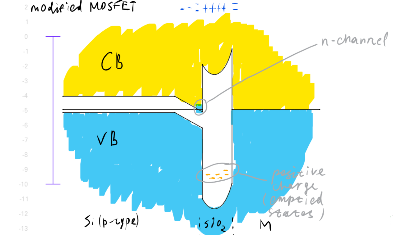
I don't know, why is the trapped charge always positive. Maybe it's even wrong. But I have a few hypotheses.
One is based on band structure of SiO2. In SiO2, conduction band extends upwars apparently into infinity. So, if an electron makes its way into SiO2 by tunneling, it can easily shoot right through (accelerated by electric field) and dissipate the gained energy in semiconductor or gate.
Valence band of SiO2 is narrow, so if an electron is extracted from it by tunneling, the resulting hole cannot shoot through SiO2 to dissipate energy elsewhere. It has to dissipate majority of its energy in SiO2. That means, it stays there for longer and has higher probability of getting stuck in any way. It can potentially get stuck by self-trapping, by being captured n an existing defect, or by creating a new defect with its own energy (is it same as self-trapping?).
Independent hypothesis is that SiO2 in a mosfet has a special set of defects, with abundance of ones that can become positive, and scarcity of ones that can become negative. It may be the nature of SiO2 itself, or may be a consequence of manufacturing technique.
These two hypotheses are not mutually exclusive, and can be in action simultaneously.