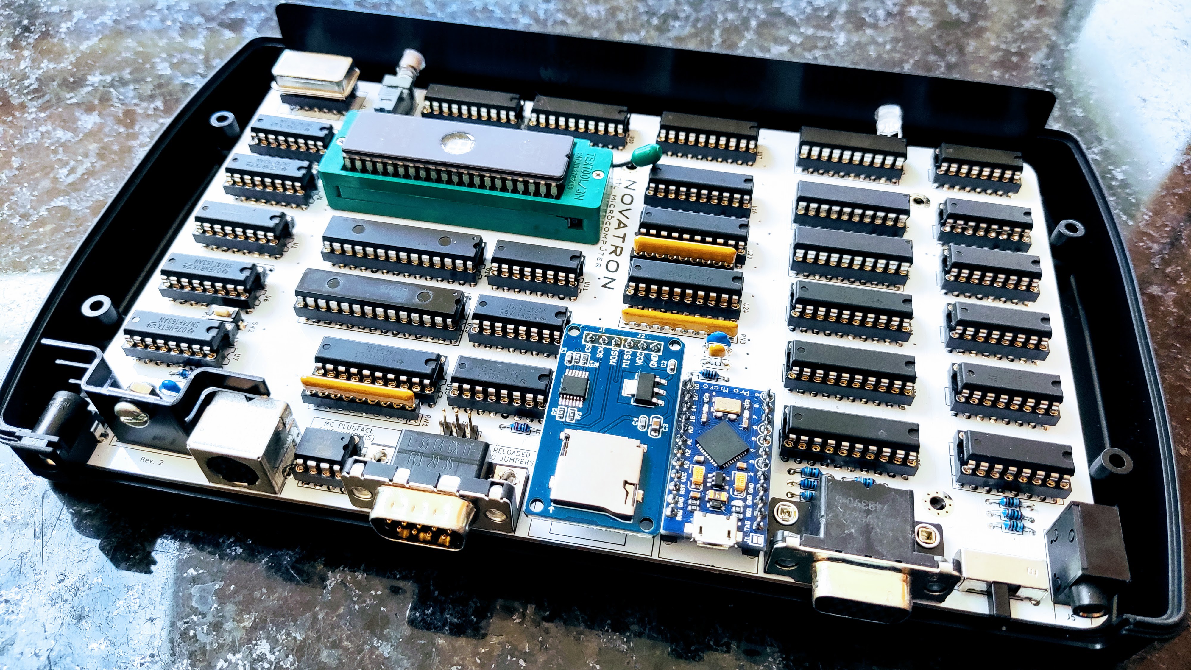
 Alastair Hewitt
Novasaur TTL Retrocomputer
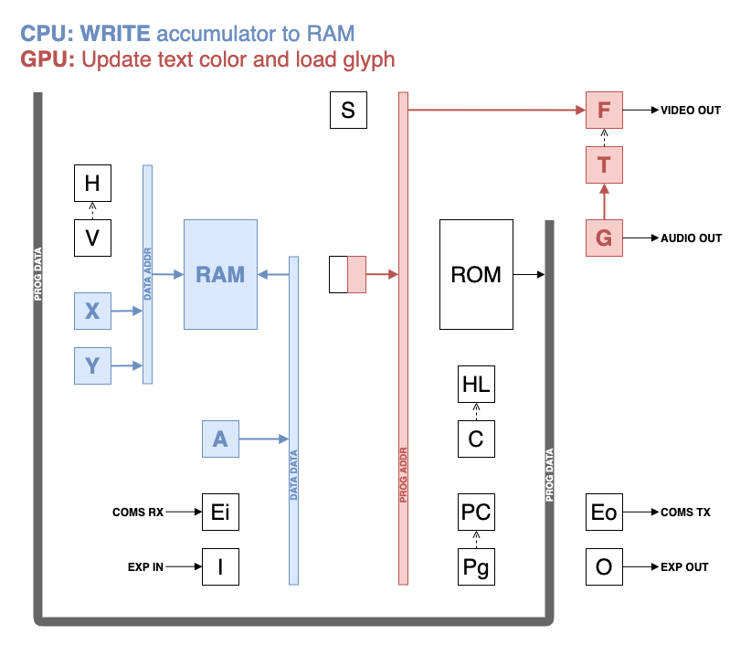
- Dual Processor CPU/GPU (Harvard Architecture).
- 33 MHz dot clock, 16.5 MHz data path, 8.25 MHz per processor (~3.5 CPU MIPs)
- 256k ROM: 96k ALU, 64k native program, 64k cold storage, 32k fonts.
- 512k RAM: 7 banks of 64k user, 60k display, 4k system.
- 76 ALU functions including multiply/divide, system, and math functions.
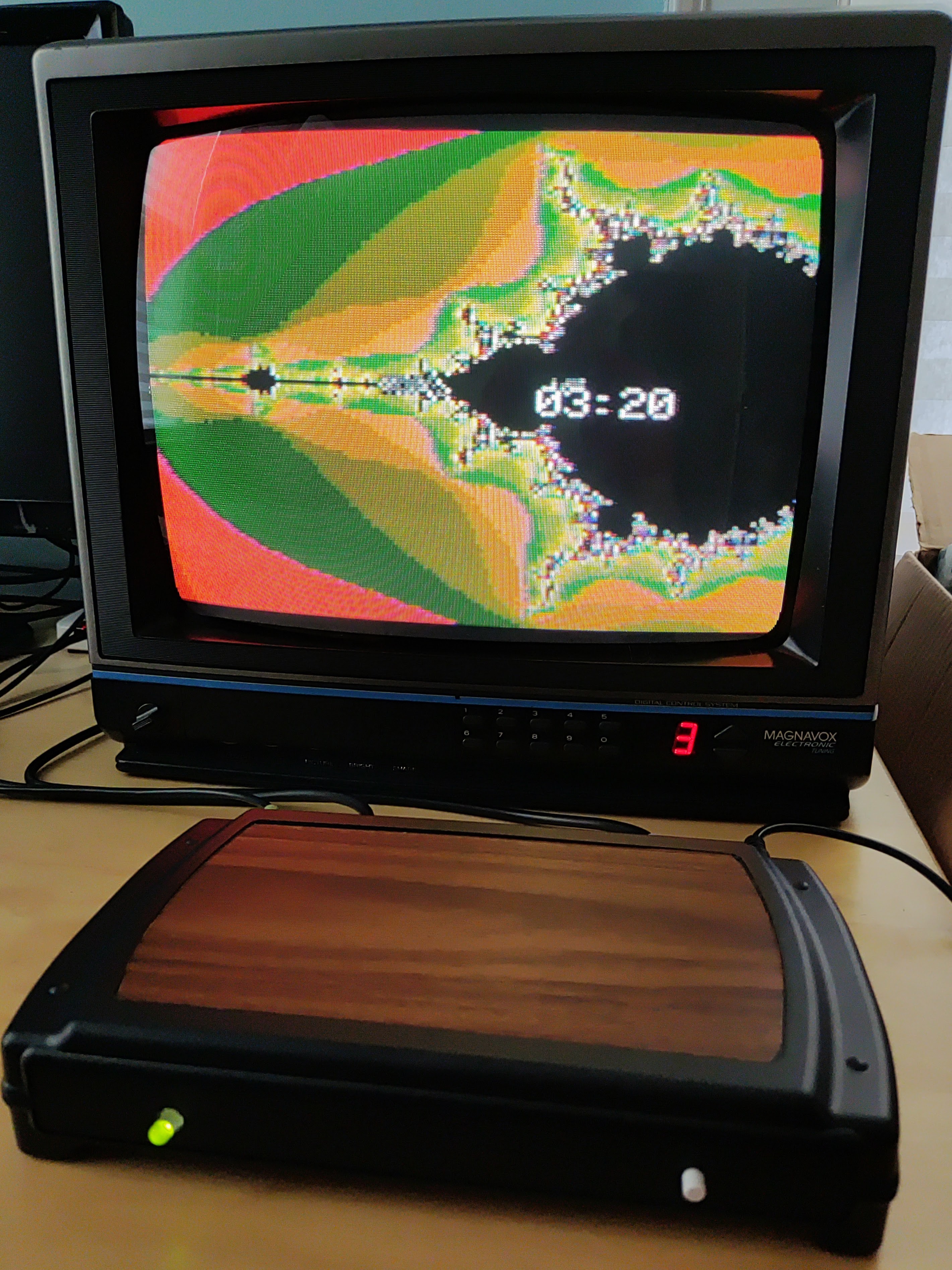
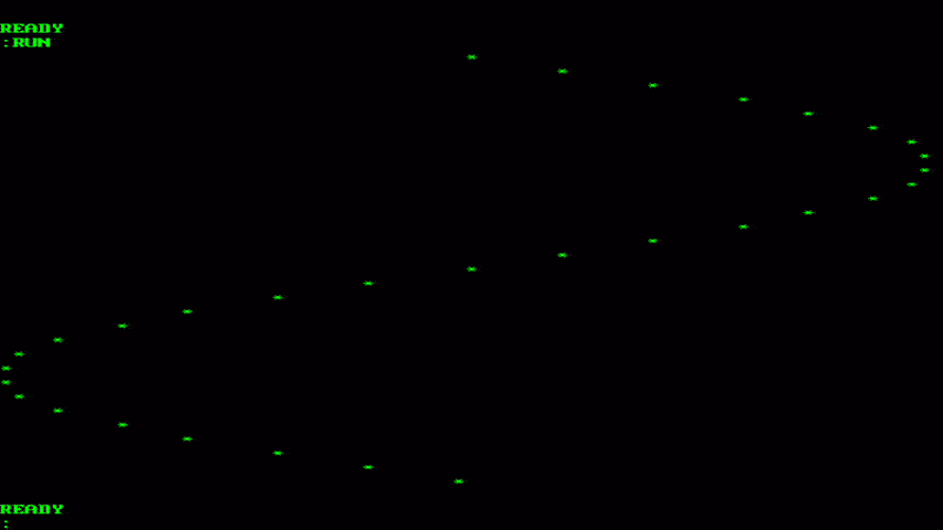
- Bitmapped Graphics: Hi-res mode up to 416x240 with 8 colors and 4 dithering patterns. Lo-res mode up to 208x160 with 256 colors, double buffered.
- Text Mode: 8 colors FG/BG, 256 line buffer, up to 104x60 using 8x8 glyphs, 80x36 and 64x48 rows using 8x16 glyphs.
- Audio: 4 voice wavetable synthesis, ADSR, 8-bit DAC, 8Hz-4.8kHz.
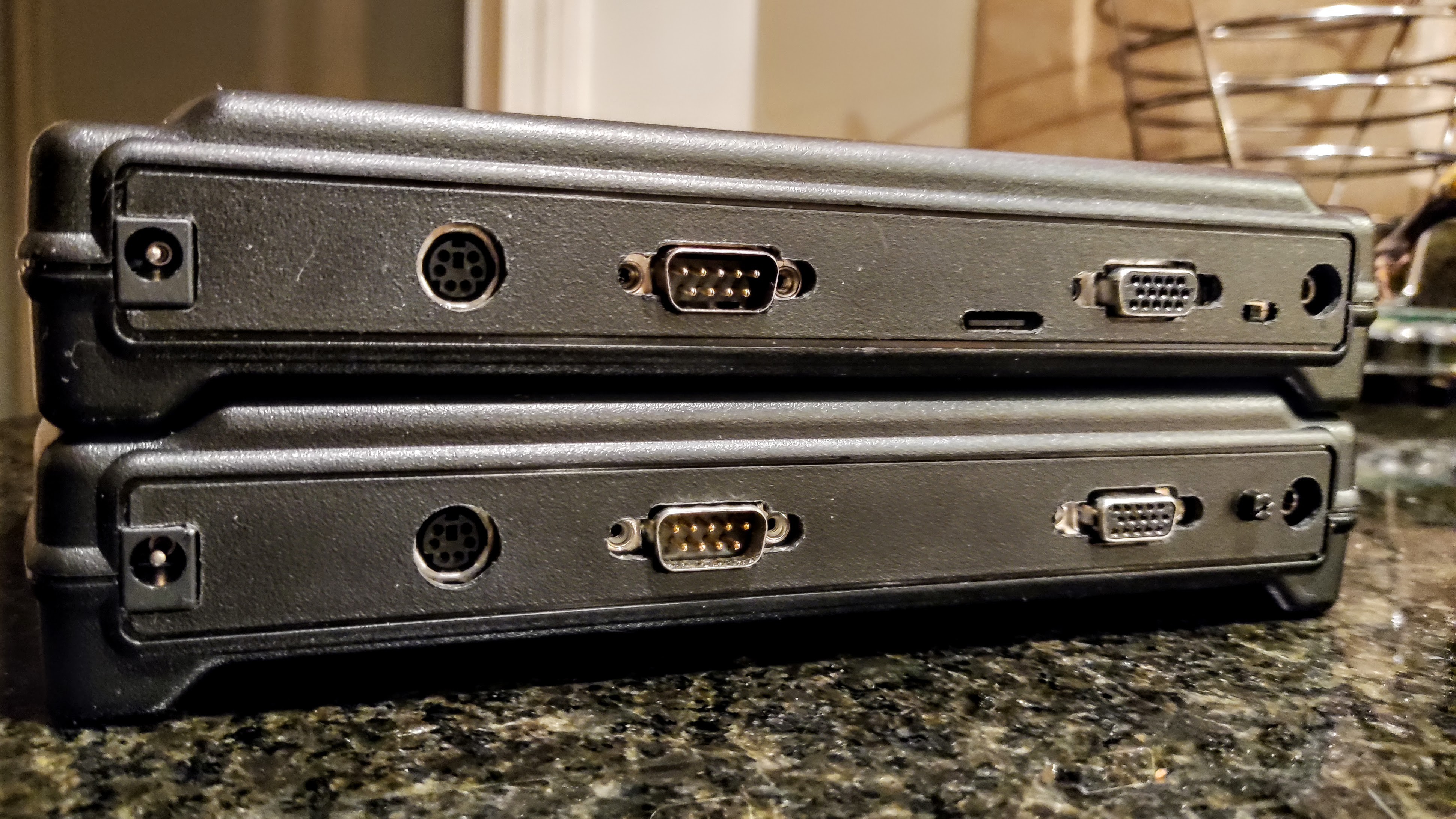
- PS2 Keyboard: Native interface built in.
- RS232 Serial Port: Full duplex, RTS/CTS flow control, 9600 baud.
- Expansion Port: 7 addressable 8-bit register ports, 4 interrupt flags
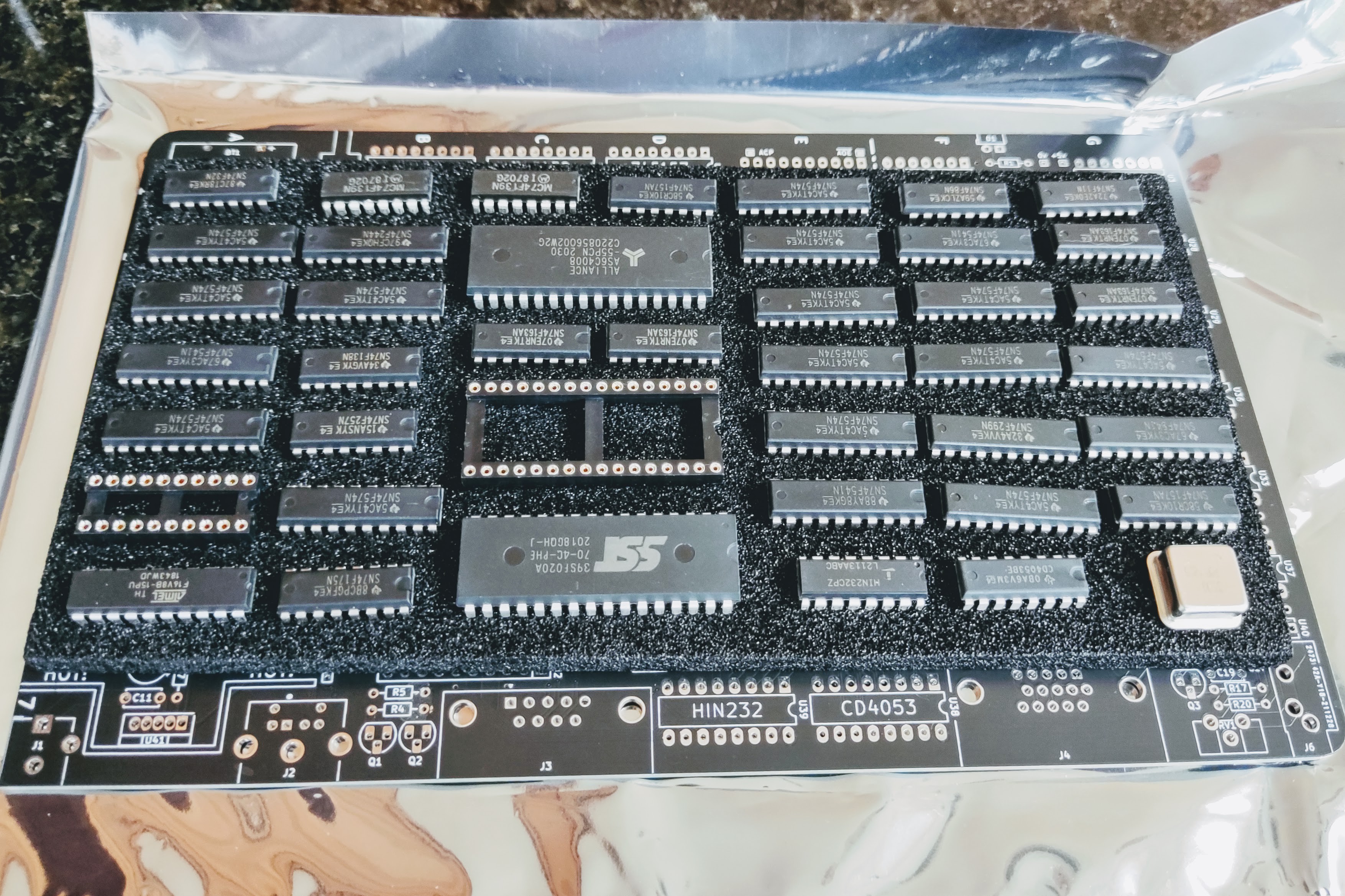
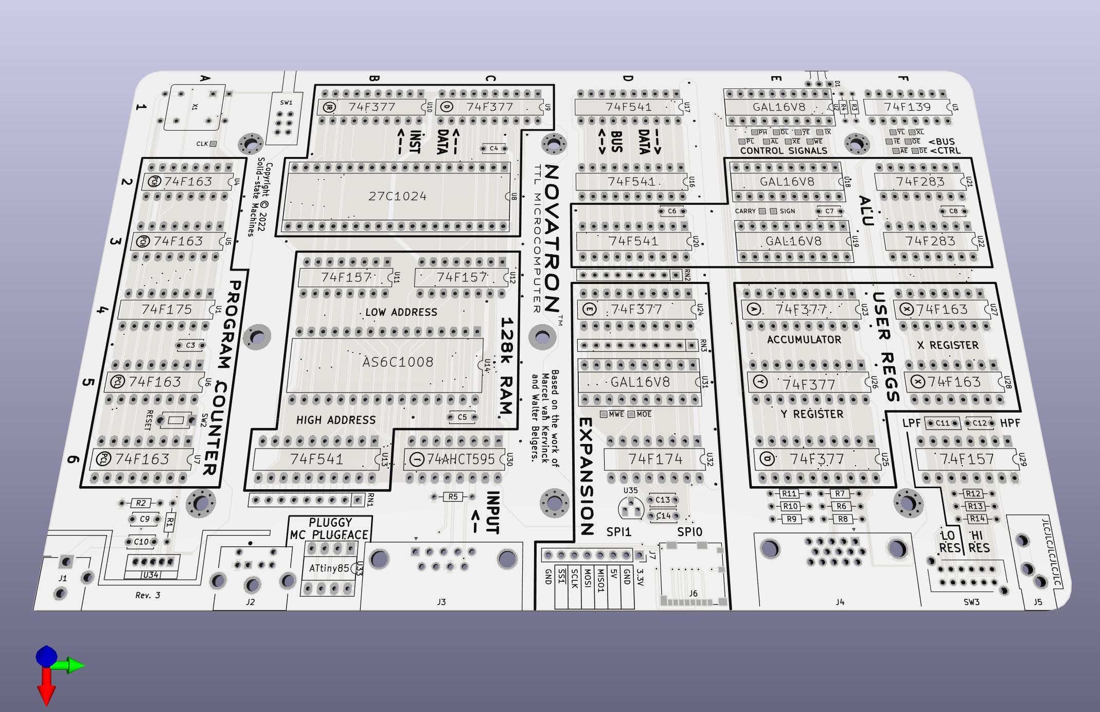
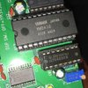
- Chip Count: 34 TTL (22 CPU, 12 GPU), 1 ROM, 1 RAM, 1 PAL, 4 analog.
- Gate Count: 1,425 (935 CPU, 490 GPU)
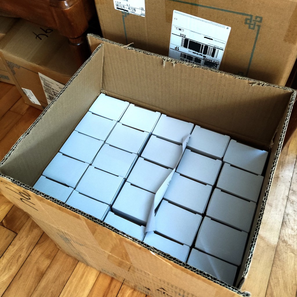
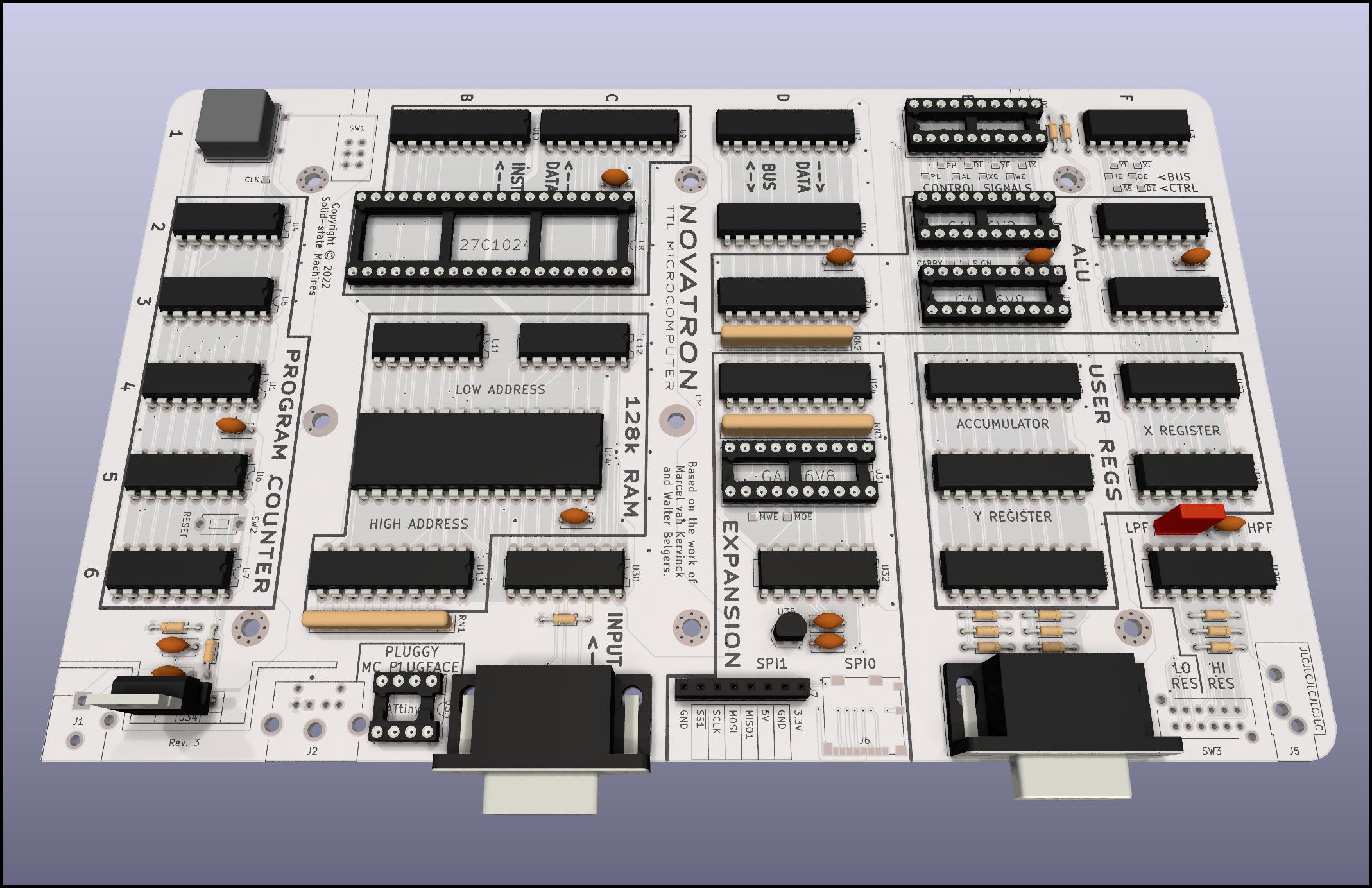
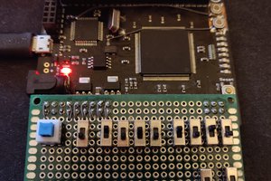
- PCB size: 8" x 5" (200 x 125mm) double-sided board.
- Power: 6v @ 1.6A (10W)
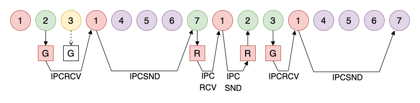
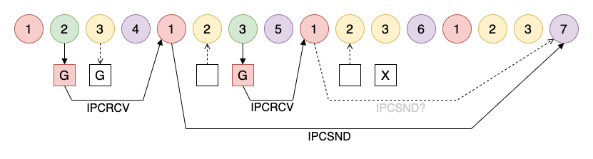
The Novasaur consists of two processing units (CPU/GPU) operating on the alternating cycles of a 4-phase clock. The 4-phase clock is driven by a 33MHz oscillator to generate a processor clock of 8.25MHz. Each processor accesses one of the two address spaces (ROM/RAM) concurrently on a memory access cycle of 60ns (16.5MHz).
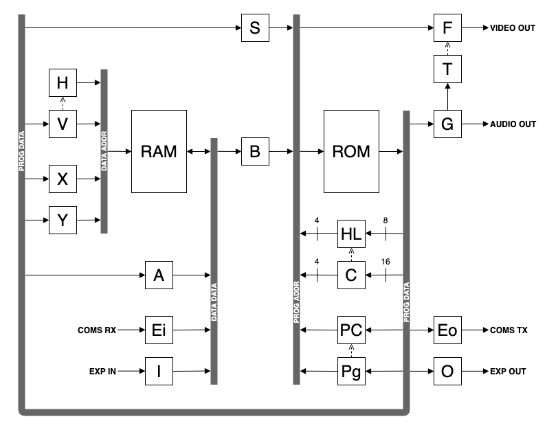
The GPU functions as a DMA controller operating in transparent mode to read the video memory and output to one of two video DACs. The first DAC generates 256 colors using three bits for the red/green, and two bits for the blue. This DAC is used for low res graphics mode where each byte of the video memory represents a single pixel.
The GPU also supports a text mode where the bytes of video memory alternate between a color byte and a code point representing a text character. The color byte is used with the second video DAC to represent two 8 color values for foreground and background. The text mode can also support a high res graphics mode with two pixels per byte of video memory.
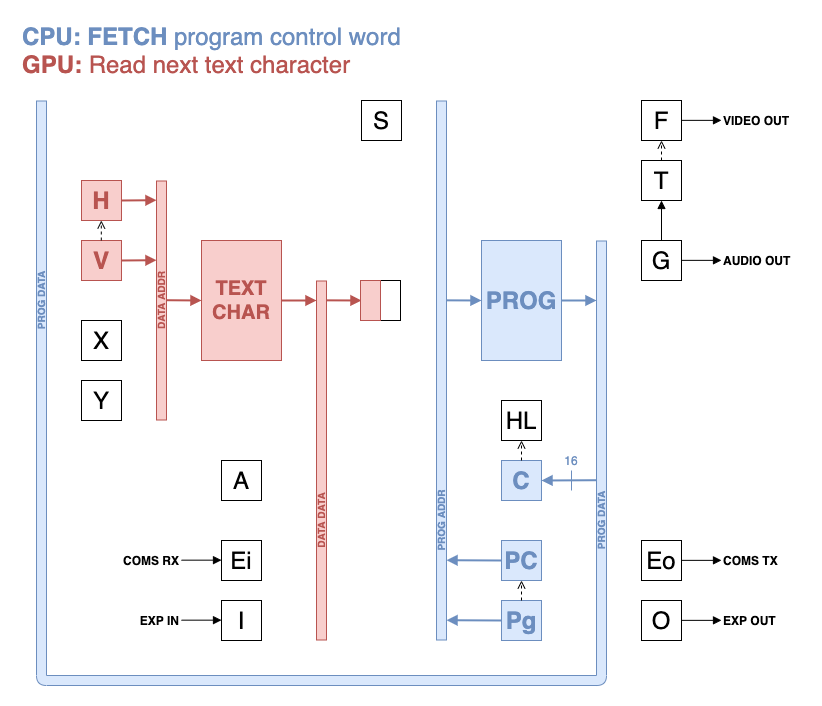
The CPU instructions use a 4-cycle sequence consisting of: fetch, read, execute, write. The fetch cycle uses a program counter to access the machine code instruction in the ROM:
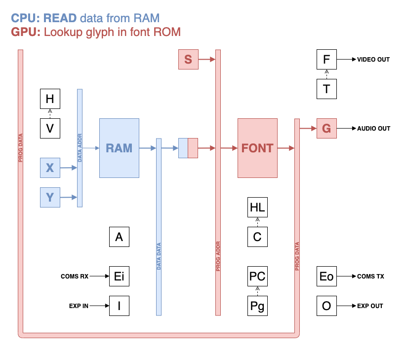
The read cycle provides access to the RAM in the indexed addressing mode.
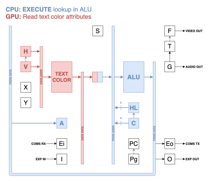
The execute cycle returns to the ROM to access the program memory for immediate addressing, or a set of lookup tables for an ALU operation.
The final cycle is the write cycle where a register is updated with the execution result and optionally the RAM in the indexed addressing mode.
Instructions take from one to four process cycles to complete: The instructions are either 8 or 16-bits, so the fetch cycle takes either one or two process cycles to complete. The ALU operations can only handle one nibble per cycle, so two process cycles are required to handle an entire byte. The NOP instruction and conditional loads, were the condition is not met, are only one cycle (no execute). On average the instructions take 2.35 process cycles to execute for a nominal CPU speed of 3.5MIPS.
The base firmware implements a hardware abstraction layer (HAL) to support a video system with up to 46 addressable video modes, a multi-voice sound synthesizer, and a dual-port UART providing a full-duplex RS232 and PS/2 interface. The operating system and user programs are executed via a byte-code interpreter providing binary compatibility with the Intel 8080/5.


 Winston Lowe
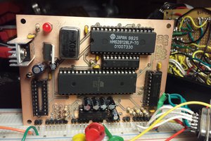
 Mars
Mars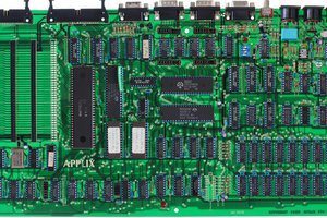
 Keith
Keith
 zpekic
I would be happy to beta test and give you feed back on the build and such (not expecting a free kit).