 Open Green Energy
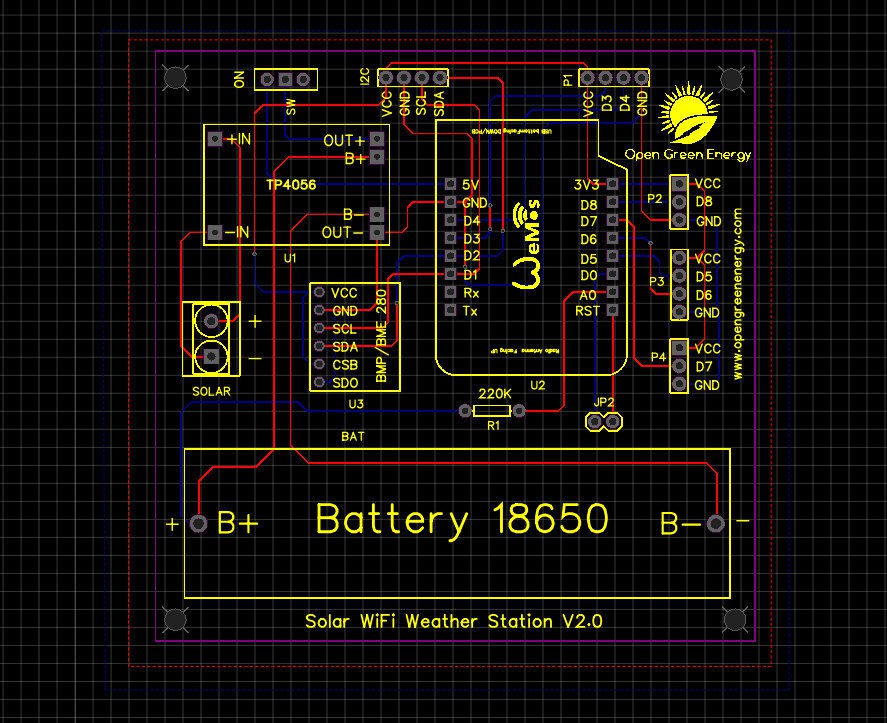
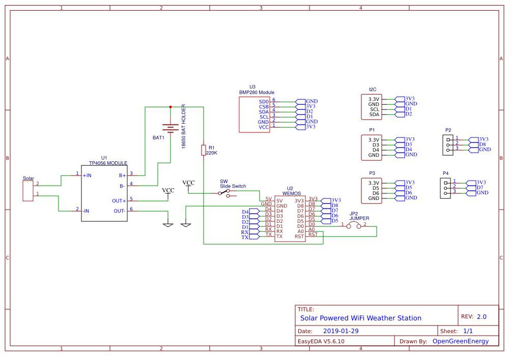
I have drawn the schematic by using EasyEDA online software after that switched to PCB layout.
All of the components you added in the schematic should be there, stacked on top of each other, ready to be placed and routed. Drag the components by grabbing on its pads. Then place it inside the rectangular border line.
Arrange all the components in such a way that the board occupies minimum space. Smaller the board size, cheaper will be the PCB manufacturing cost. It will be useful if this board has some mounting holes on it so that it can be mounted in an enclosure.
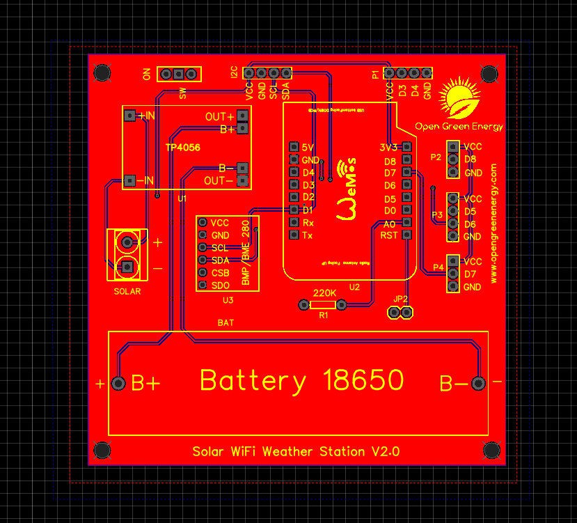
Now you have to route. Routing is the most fun part of this entire process. It’s like solving a puzzle! Using the tracking tool we need to connect all the components. You can use both the top and the bottom layer for avoiding overlap between two different tracks and making the tracks shorter.
You can use the Silk layer to add text to the board. Also, we are able to insert an image file, so I add an image on of my website logo to be printed on the board. At the end using the copper area tool, we need to create the ground area of the PCB.
Now the PCB is ready for manufacturing.
Discussions
Become a Hackaday.io Member
Create an account to leave a comment. Already have an account? Log In.