At the core of all power supplies is a transformer. It is central to the design and dictates the form and function of everything around it. A home brew design imposes additional requirements. Without specialized tooling and winding materials (e.g. Litz or foil wire, etc.) the design must also be constructible. Given this, my criteria were that the transformer must be:
- Manufacturable
- Efficient
- Simple
- Reliable
From earlier work I knew that a center tap secondary is not practical due to the voltage gradient and turn-turn capacitance.
In a center tap secondary, the voltage measured across the legs is twice the output voltage. So a 200V secondary actually has 400V across the entire winding. In high frequency transformers this, combined with the turn-turn capacitance becomes a serious problem that results in significant ringing. Here’s an example:
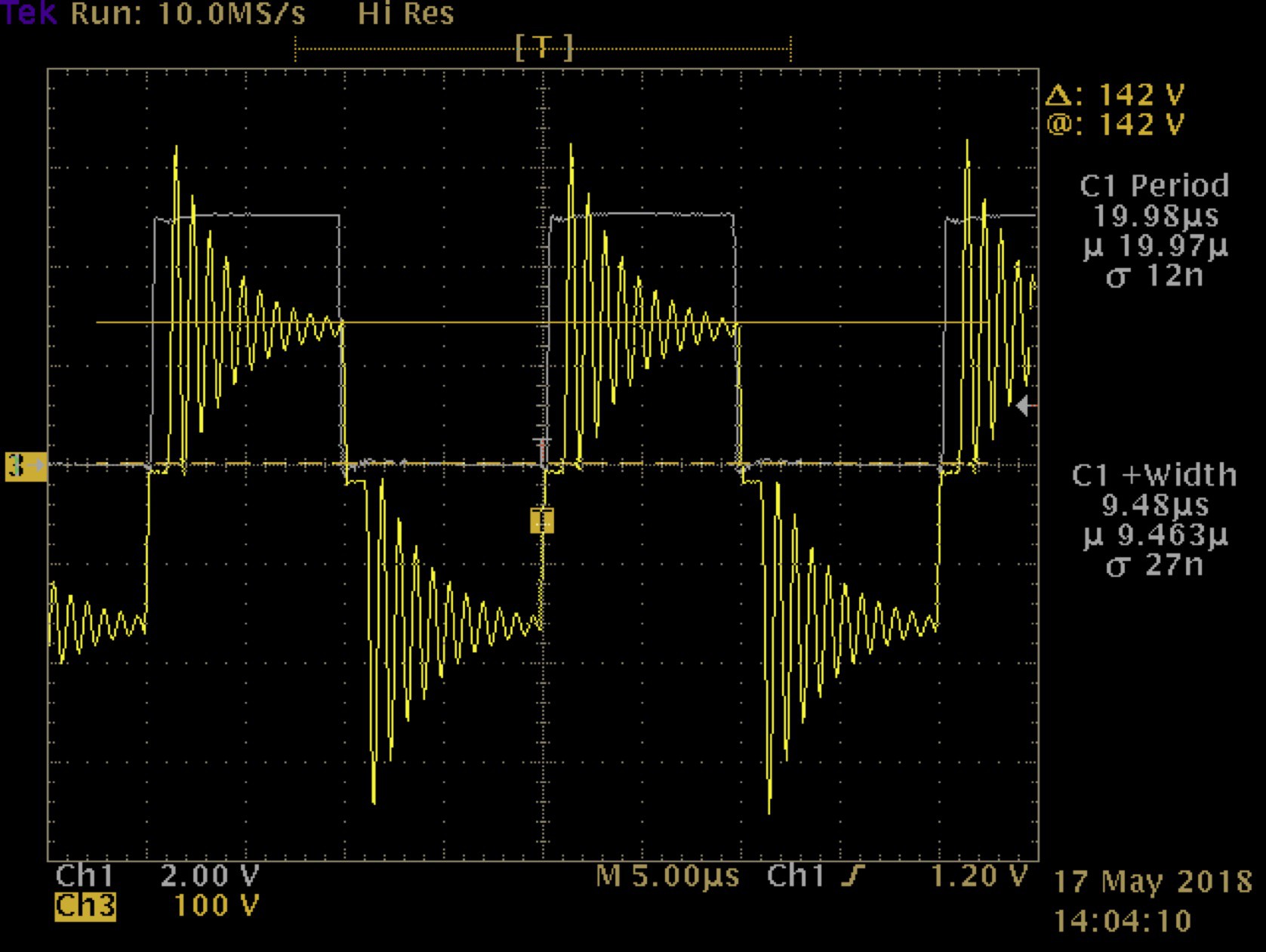
Note the cursor value and the scale for channel 3 - 100V! Professionals get around this with lower capacitance magnet wire and special winding techniques that can only be done by machine (e.g. Bank).
Which is a shame since a center tap requires only two rectifiers instead of four. That may not seem significant but consider the consequences: space, dissipation, materials. In this design if a CT were viable I could have ditched the heatsink and likely used two SMD diodes saving space & halving the dissipation.
Decision 1: single winding secondary.
A center tap primary is possible and that would allow the use of a half-bridge - again saving significant space and halving dissipation. But there are drawbacks:
- Window utilization is poor - each half winding is only doing work half time.
- A larger core size would likely be required given the size of the winding - 2 turns of 20 AWG 10 strands becomes 4 turns.
- Terminating the center tap would be problematic.
- Greater chance of staircase saturation: any imbalance in each half winding (due to construction) creates a flux imbalance which over successive cycles walks the core into saturation.
Decision 2: single winding primary.
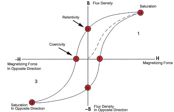
An inverter acting as an AC power source must be capable of handling large currents and supporting surge power well beyond their continuous rating. To do this the transformer must have a high power density and this requires operating it across the full BH loop in quadrants 1 & 3.
This is related to the single vs. center-tap primary discussion but emphasizes the power handling requirement of the transformer. To operate the transformer in this manner requires either a half or full bridge; but the prior discussion already discounted the half bridge due to manufacture concerns.
Decision 3: full bridge.
Most switching power supplies regulate thru some form of modulation - either the switching frequency, duty cycle, or both. Without a center tap secondary the conventional approach to regulation via the use of an output inductor to prevent the transformer core from resetting during off time isn’t practical. A current fed primary topology is a possibility but adds inductors & switches, introduces more losses, complicates the design, requires more space.
Decision 4: no regulation.
These decisions support the design criteria: a design that is manufacturable, simple, reliable, and (theoretically) efficient. The transformer can be operated at a high, constant, duty cycle, utilizing the full BH loop and achieving good power density. The complexity of a control loop is eliminated. But this shifts some burden to the rest of the design, both in front of and behind the transformer:
- A full bridge will be used, doubling the space requirements and losses.
- A full bridge rectifier is required, also doubling the space requirements and losses.
- The secondaries will track the input voltage according to their turns ratio and both limit the input voltage operating range and require components with higher voltage ratings.
- A method of regulating the AC output voltage will be required. Fortunately precise regulation isn’t necessary.
With the transformer design and operating modes set the remainder of the inverter design is relatively straight forward. The gate drivers and current sense circuit are placed on a vertical mount daughter board to conserve space and keep the gate drive loops small. This is an idea I’ll likely carry forward to higher power designs using heavier copper on the main power board (in fact expand it so that all logic resides there).
The 2oz limitation on maker PCBs forces some compromise in the layout. Ideally the gate drive card would reside in front of the transistors instead of between them and the transformer. I couldn’t do that because I needed all the copper area I could get to feed energy to and return from the bridge. The card, with its pins and gate drive traces would interfere.
I specifically selected the Ohmite heatsinks because of their mounting flexibility. I was really concerned that the parasitic inductance in the MOSFET leads combined with a 2oz maker PCB would cause grief for the monolithic gate drives. Mounting the transistors at minimum height significantly reduces this. So much so that even under hot over-current / over-load conditions the design doesn’t need protective circuits for the typical VS or COM below ground problems.
Discussions
Become a Hackaday.io Member
Create an account to leave a comment. Already have an account? Log In.