 Mark Omo
As the maker community continues to expand, there is a growing demand for entry-level tools that are affordable, and chiefly, simple. The basic tools of electronics development haven’t changed in a long time, but much like the TS100 iron made precise soldering more accessible, we aim to make signal analysis more accessible through our entirely self-contained oscilloscope and probe: The Probe-Scope. At its core, the Probe-Scope is a compact single channel oscilloscope with all the acquisition hardware contained along the cable (either in the probe body or into an enlarged USB connector, we’re still working on that detail).
Architecture
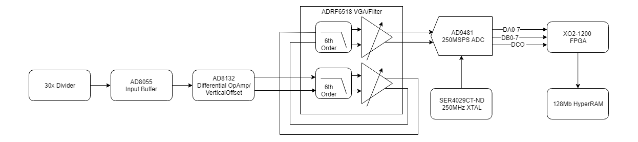
The Probe-Scope’s architecture can be described in three sections: the input divider and buffer, the programmable-gain amplifier (PGA), and the acquisition hardware.
Input Divider/Buffer
The input signal first goes through a fixed 30x divider, the output of which is buffered by a high-speed op-amp, giving the probe a ±15V range, ±150V in x10 mode. Then the signal goes to a differential op-amp configured to sum the signal with an offset signal from a DAC, before finally going into the gain settings in the PGA. One of the most critical parts of the frontend is keeping noise low: total noise is proportional to the bandwidth that you measure over, and we’re targeting a bandwidth of over 50MHz, meaning any noise on the frontend will have a much greater impact than at a lower bandwidth. (For reference, the largest single noise source is the input resistor divider.)
Programmable-Gain Amplifier
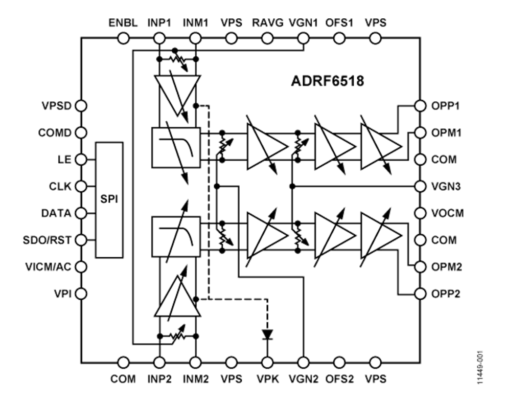
The PGA is a single ADRF6518 that contains both a programmable-gain amplifier and filter, with two identical paths. It serves two functions: boosting or attenuating the input signal in preparation for the ADC and performing anti-aliasing. We take advantage of the ADRF6518’s two paths by looping the signal through twice, to achieve a very sharp anti-aliasing filter response. The filter’s response is effectively a 12th order filter (from two sequential 6 pole filters), providing 240dB/decade of rejection and allowing us to reach 50Mhz of (noise free) bandwidth with only a 250MSps ADC.
Acquisition
To sample the signal in our digital section, we have selected the AD9481, an 8-bit 250MSps ADC which has an ENOB (equivalent number of bits) of 7.9 bits, providing high performance. The ADC’s output is fed into a MachXO2 FPGA, which in turn stores it into a 128Mb HyperRAM, providing 16Mpts of memory. The triggering is all digital, handled by the FPGA.
Not shown in the diagram is a PIC32MZ EF which is also connected to the FPGA. After all the data is acquired for one trigger, the PIC32 reads it off the HyperRAM (through the FPGA) and then transmits it over USB to a PC for display. The PIC32 also controls the vertical offset DAC, communicates with the ADRF6518 via SPI, and sets the triggering on the FPGA.
Discussions
Become a Hackaday.io Member
Create an account to leave a comment. Already have an account? Log In.