 James Rowley
While designing our Digital Test PCB (which I'll be posting about in detail in a day or two), I decided to take a couple screenshots of the board as I worked on it, thinking it might be fun to see how it comes along. In the center of the board is the MachXO2-4000 FPGA, with our PIC32MZ2048EFH processor on its left port, the AD9481 ADC on the bottom, and a 128Mbit Cypress HyperRAM on the right port.
I start by defining the board size and bringing in all the components from the schematic, then placing the connectors and major components:
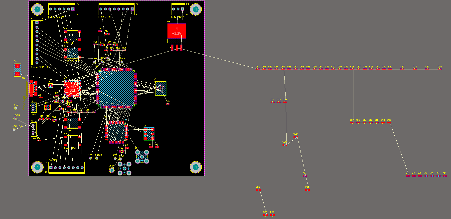
The board is 100x100mm as that's the cutoff for PCBWay's lowest price. I organized everything around the FPGA since it's really the hub of all our signals. You might notice that the final version has a few more connectors - since we're in the early development phases, it's a fairly fluid process, and Mark thought of some more nice-to-have features so I just went ahead and threw them on.
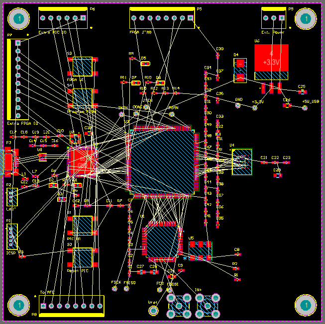
Next, I get all the decoupling capacitors next to their associated ICs (with some old-fashioned pen-and-paper action) and roughly place minor components:
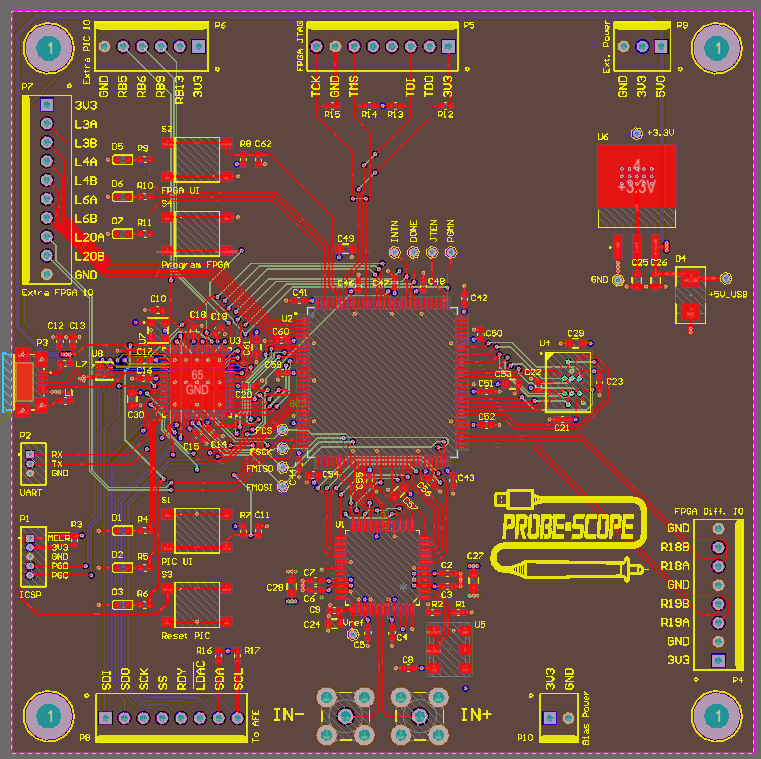
Now for the "draw the rest of the owl" step, I route everything and finalize component placement. This board took me roughly 10 hours to route (very roughly, I should have timed it). I put a ground plane on layer 1 and a power plane on the bottom, so I tried to avoid those as much as possible but completely avoiding them wasn't practical. I'd have gone into a bit more detail with the pictures, but it's really just drawing lines that can't cross for hours until it's done. Here's the result:
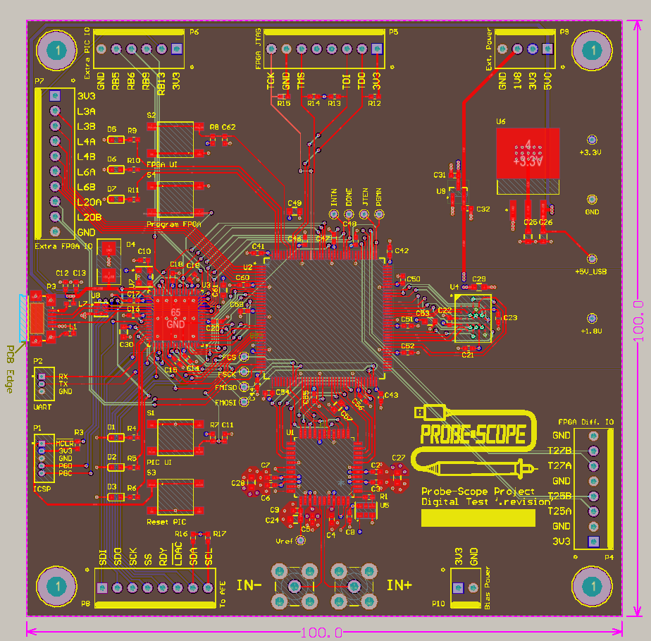
Of course, there's always still a few tweaks to be made. I made the power test points a little more logical, moved our debug differential IO to the top port which has true differential drivers, and made a single trace going under the RAM a couple mils thinner as the manufacturer informed us that there is a wider clearance between BGA pads and other copper in the normal process (it would have cost around $400 instead of about $50!). We also realized just in the nick of time that we required the 1.8V version of the HyperRAM part in order to get the full speed which we needed, so a 1.8V rail was added for that.
So here's the final design we sent to the manufacturer:
On the final board, I'm planning to get a timelapse of the whole layout process (unfortunately none of this layout will be reusable as compactness is a priority). You can check out the board on our GitHub page, and I will be writing another post about its design and function in a couple days. Hopefully we'll have them built up a few days after that!
Discussions
Become a Hackaday.io Member
Create an account to leave a comment. Already have an account? Log In.