 Brandon Reinhart
I've mostly finished my Arduino sketch for generating the instruction words that will drive the control logic in the computer.
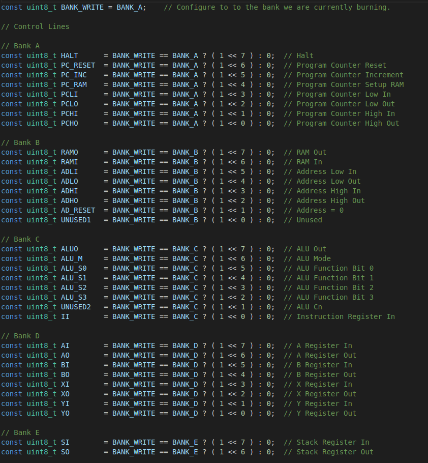
We define a bank as an EEPROM with 8 output lines. With that in mind, we can define as many control lines as we want to support:
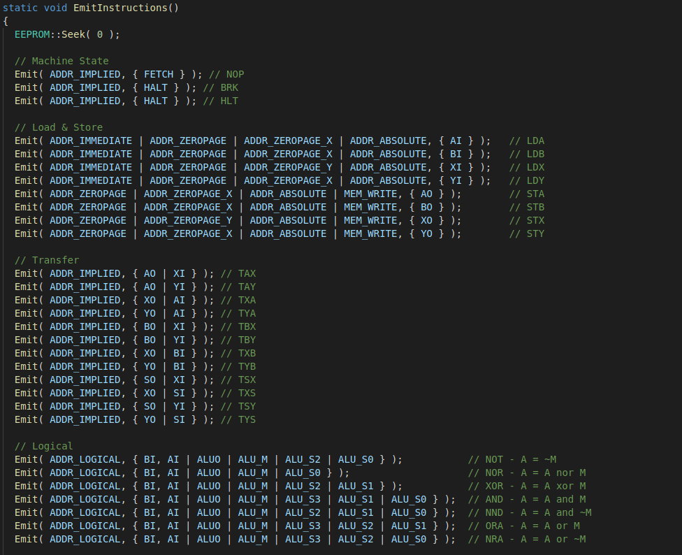
We can define an instruction as a pair of flags (defining addressing modes or that we want to write memory) with a set of operations per time step:
Since we only define the value of control lines for the bank we're writing, we can fold an arbitrary number of control lines into the single byte that represents this EEPROM's output lines. This lets the stepwise definition of each instruction be very readable inline. I liked this approach better than the giant table I was using before.
Addressing modes are drawn from the 6502, which I want to learn to implement in more detail:
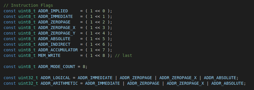
There are still more modes to support.
The Emit function will output the byte stream that implements the instruction for each addressing mode. The opcode is the address of the first timestep of that instruction for a given addressing mode.
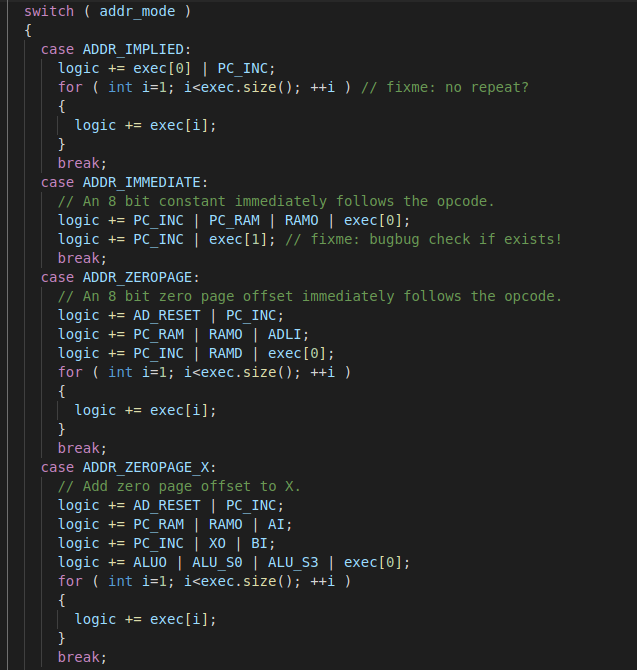
Each addressing mode outputs a series of required steps to get the correct address. Not saying the above code is correct. It hasn't been tested yet (this sketch wasn't developed using a unit test rig).
Some straightforward write logic drives the hardware:
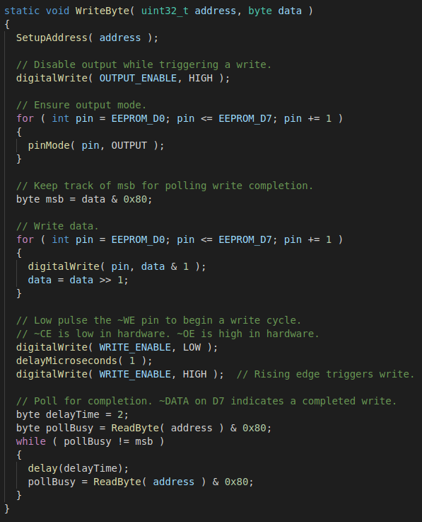
These EEPROMs use a method of writing back the inverse of data bit 7 to indicate a completed write. This particular EEPROM also cycles data bit 6 while a write is active.
The end result is, for every EEPROM, a set of steps at an address that is the opcode + timestep.
I also write the HALT step to every position on the EEPROM as a clear value. This will stop execution of the computer if we ever try to use an unimplemented instruction or some unwritten word in the EEPROM.
Here is an example with LDA imm (load register A, immediate), which is opcode 0x18:
             t0    t1    t2    t3    t4    t5    t6    t7
BankA: 18:   30    20    10    80    80    80    80    80
BankB: 18:   80     0    80     0     0     0     0     0
BankC: 18:    0     0     1     0     0     0     0     0
BankD: 18:   80     0     0     0     0     0     0     0
In this case, t0 sets bits on banks A, B, and D as the first step of an immediate mode instruction (advance the PC to get the argument). At t1 bits are set on banks A and D which transfers the value of the argument in memory to the A register. At t2 we fetch the next instruction. The rest of the timestamps (t3 ... t7) are invalid and will drive the HALT line (0x80) on bank A if accessed.
With this framework in place I just have to wire up the control lines, author the remaining instructions and memory addressing modes, and burn the EEPROMs.
Several instructions outstanding require new hardware components. I need a processor status register (for carry, zero, etc) and I'd like to add a shift register.
Discussions
Become a Hackaday.io Member
Create an account to leave a comment. Already have an account? Log In.