One day I was playing with my phone, and a drop of water landed on my screen. That little water drop formed a little microscope, so I coud see my phone screen pixels. That water started this project, because after that I wanted to look more and more smaller object on it. I decided, I want to photograph what see on that screen.
I work in the display industry, but I never saw with my own eyes how a screen really works. I was interrested about the electrical side of a screen, like how they could operate that much pixels in the size like phone.
Because of my work I saw some thin firm transistors on a layer of screens, and also a bit of research I knew what to look for.
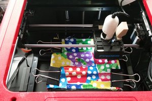
I was thinking about how to make a cheap big magnification microscope. It was not easy, but I rememberred the CD readers head has a really good optic in it. I started playing with my Iphone screen and a cd reader head, I could saw much more details then before, but that was not enough form me then. After I tried with the same optic with my Iphone 7 plus camera so I started photograph. I had a cheap chines LCD touch screen for an arduino uno what I never used for any project, so I made a sacrifice. I used the cheap screen back light to light the screen then placed the microscope optic, but the result was not the best. I only could see the red, green and blue pixels, nothing else.

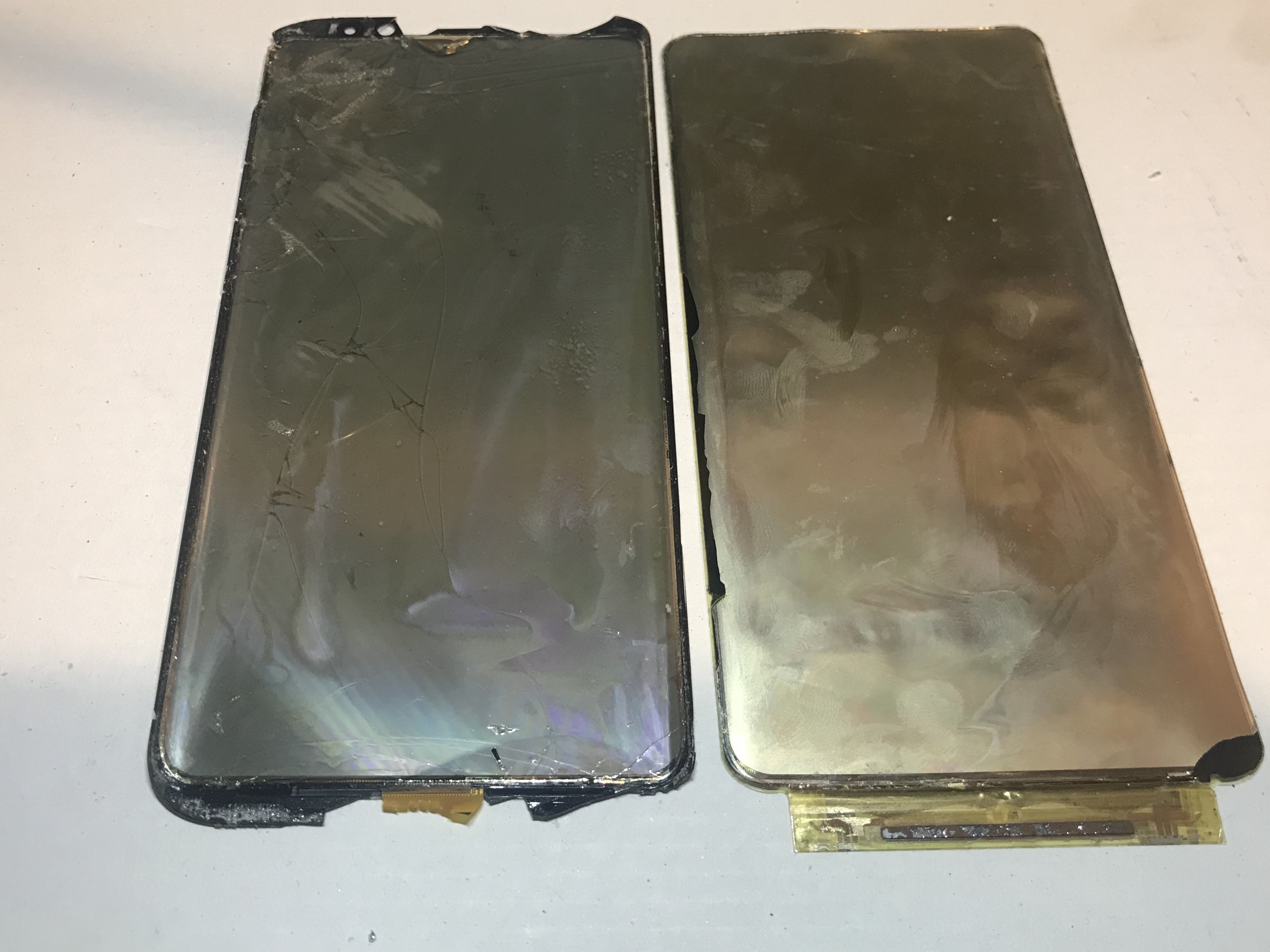
After a lot of struggle, I found out the screens usualy built from two glas layer between the liquid crystals. The top glass has black masking where they want to hide the controll circuit. That mean between two sub-pixel it is black area. The problem with this the transistors and the controll lines are between these pixels, so I could not saw them.
Then I disassembled the screen and removed the front LED backlight and all the polarizer films from the front and the back also.
With this I coud see the transistors and the lines from the back side, but the problem was still that black masking around the pixels I tried to see from the top.
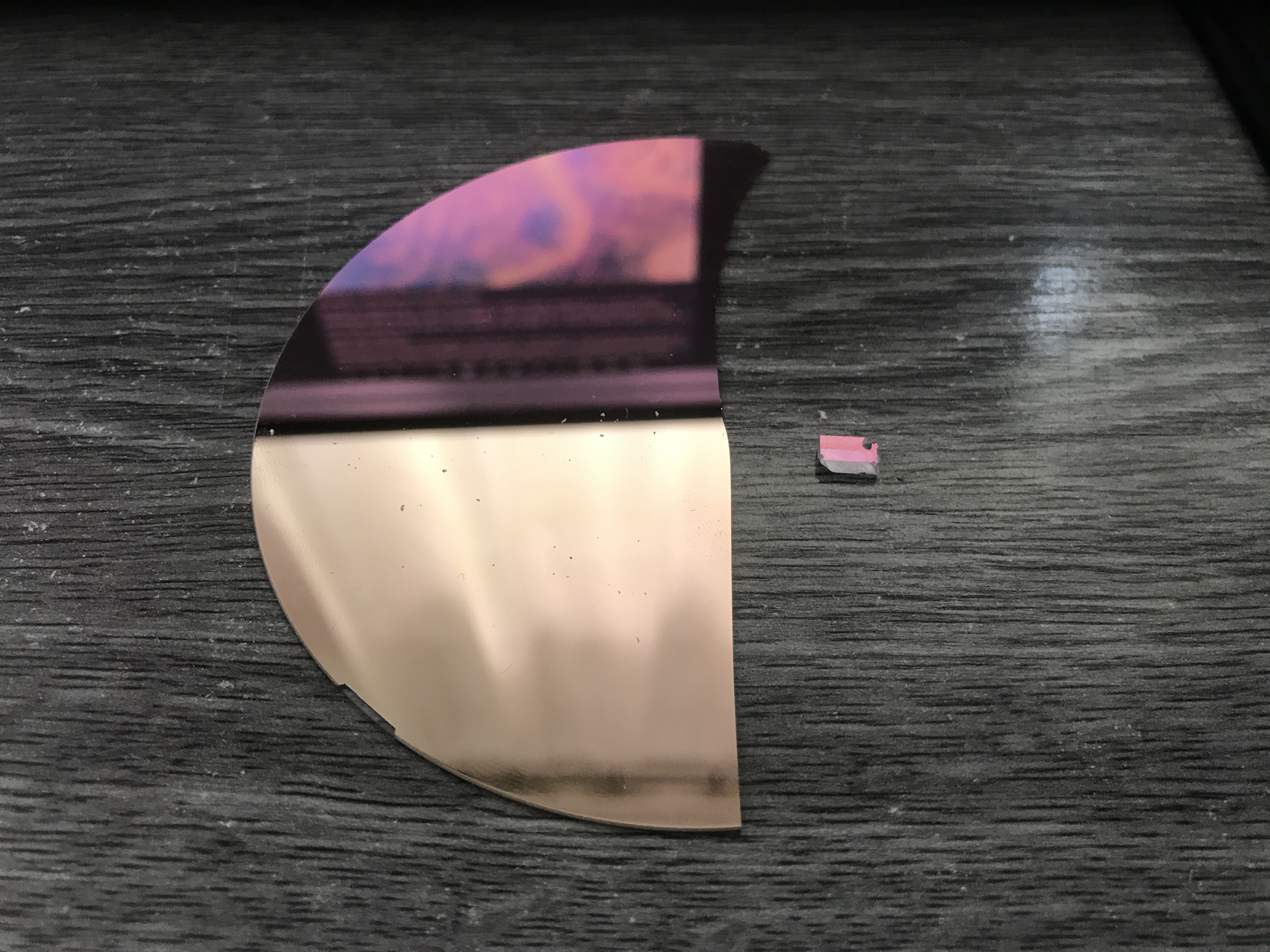
I had no chance and had to try separate the top and the bottom glass layer. It was feirly easy with a sharp blade.
Then lets see what cold I achieve with this:
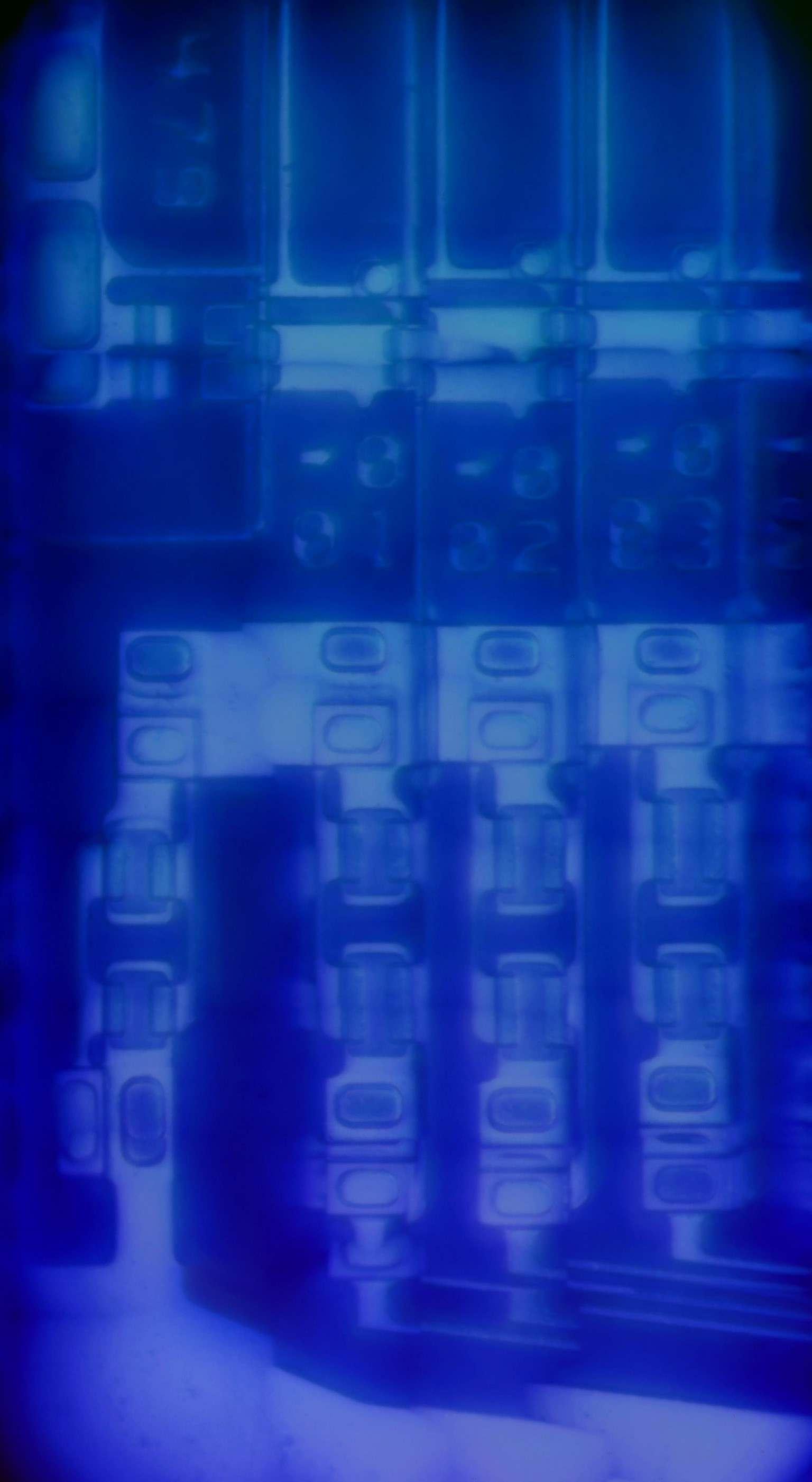
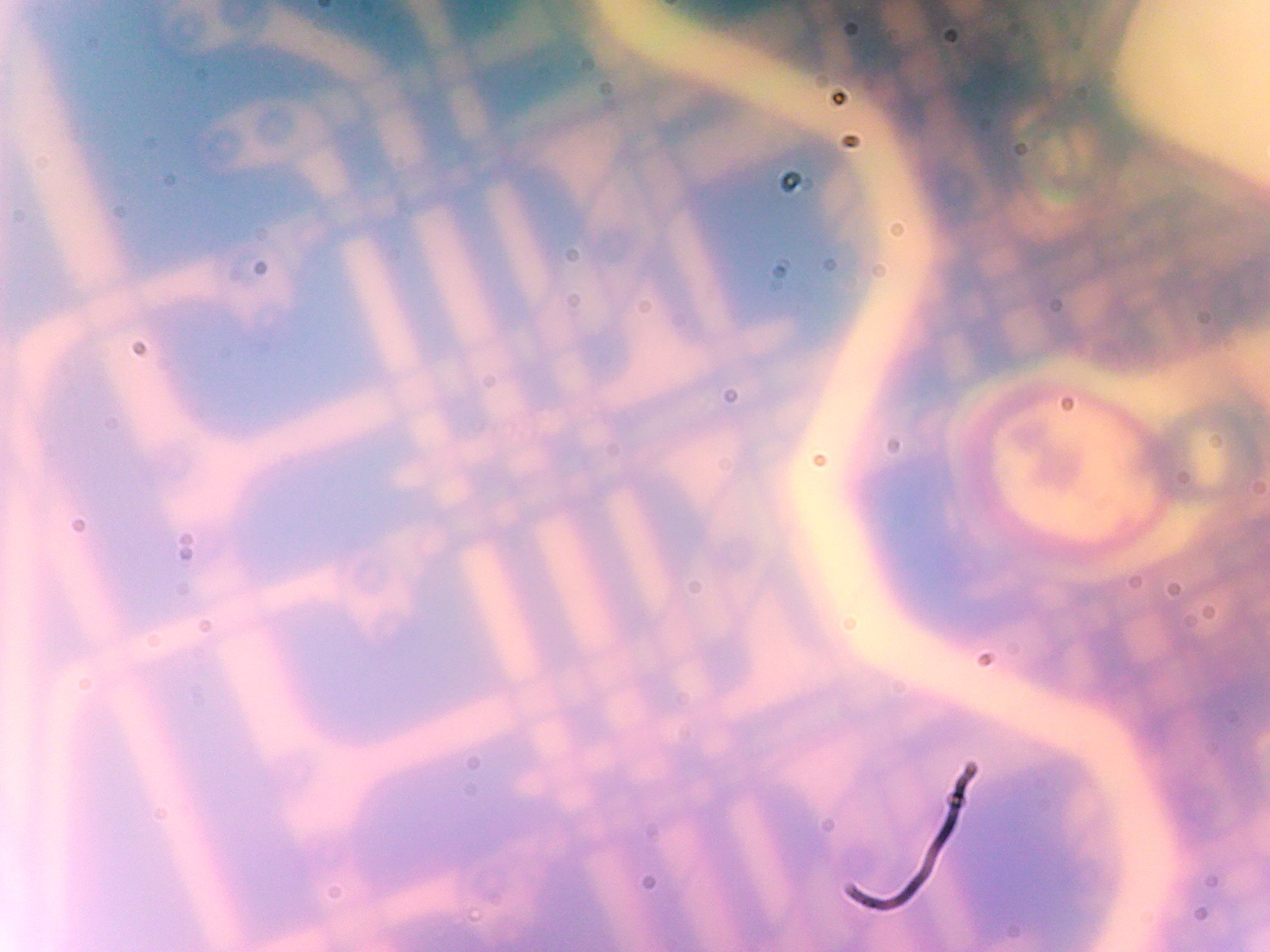
Not so bad right? I achived this with a CD reader head optic a RGB led and my phone camera.
The CD reader head has a good option because it is reflective optic, so it usually has a laser what is shining down to the surface then the light comes back to a photo transistor, and that how it detect data on CD surface. This point I replaced the laser with a RGB led and I removed the photo transistor also and ther went my phone camera.
This picture was created from several picture combination, that why it is not perfect.
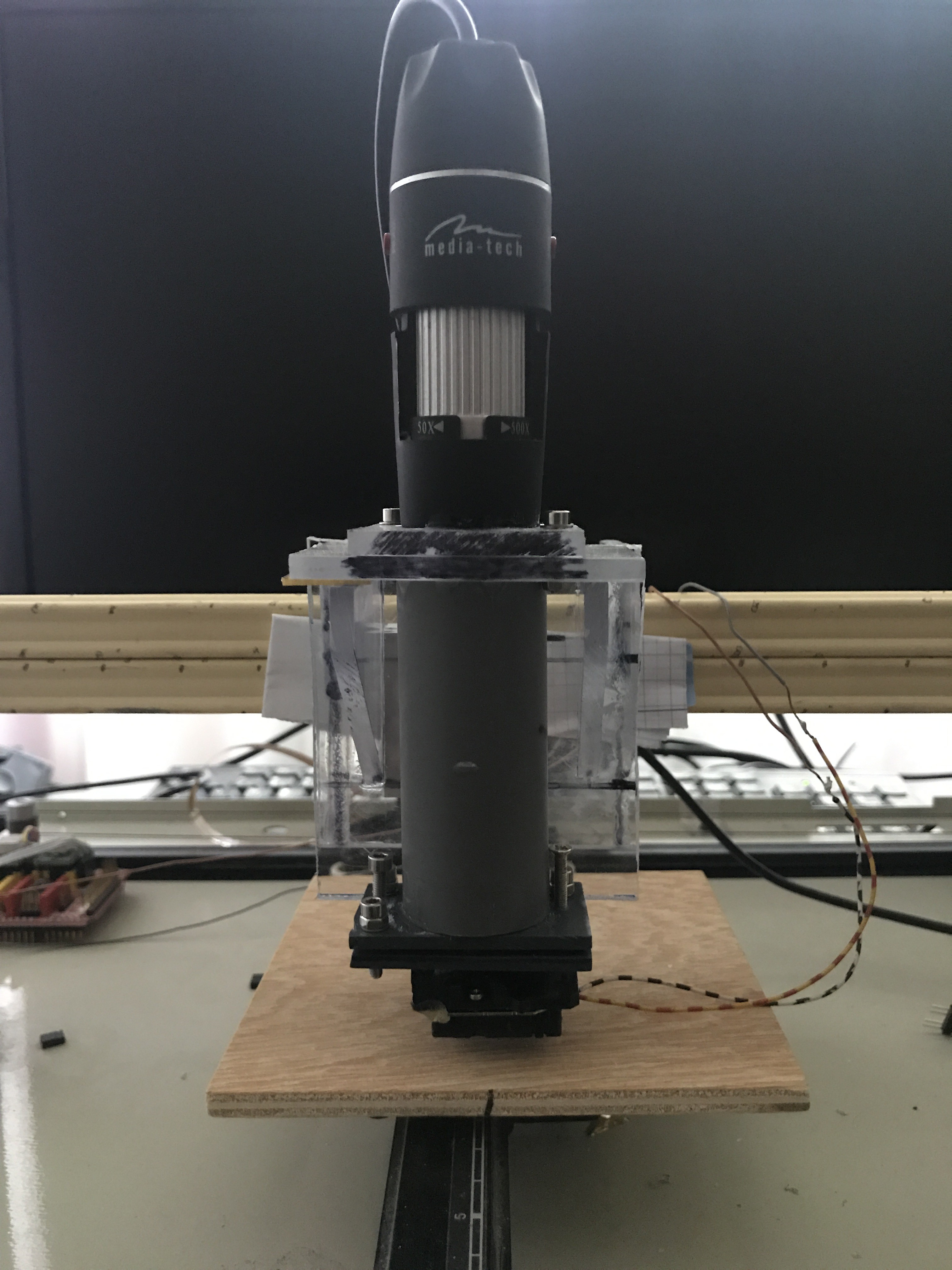
Then I decided to improve the system by adding X - Y movement too, so I could search for interresting parts.
I had an old pen plotter what long time I was looking for where can I use it.
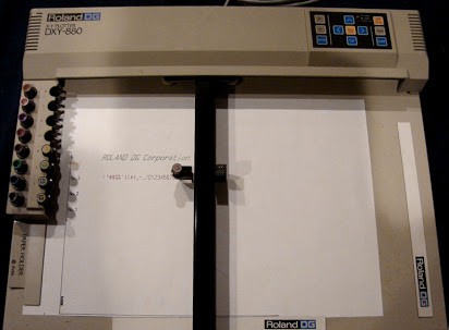
I modified the controll electronic with a modern arduino CNC shield, so then I can write software for it.
Also needed USB camera instead of my phone camera, so I was looking for a cheap solution and I found a usb microscope camera, I knew it is not so great, but it has magnification already and I did not needed big resolution, you will understand it later why.
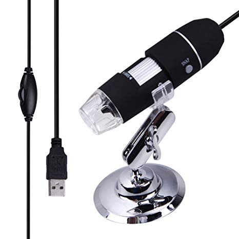
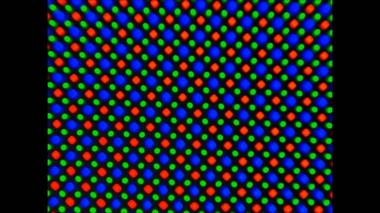
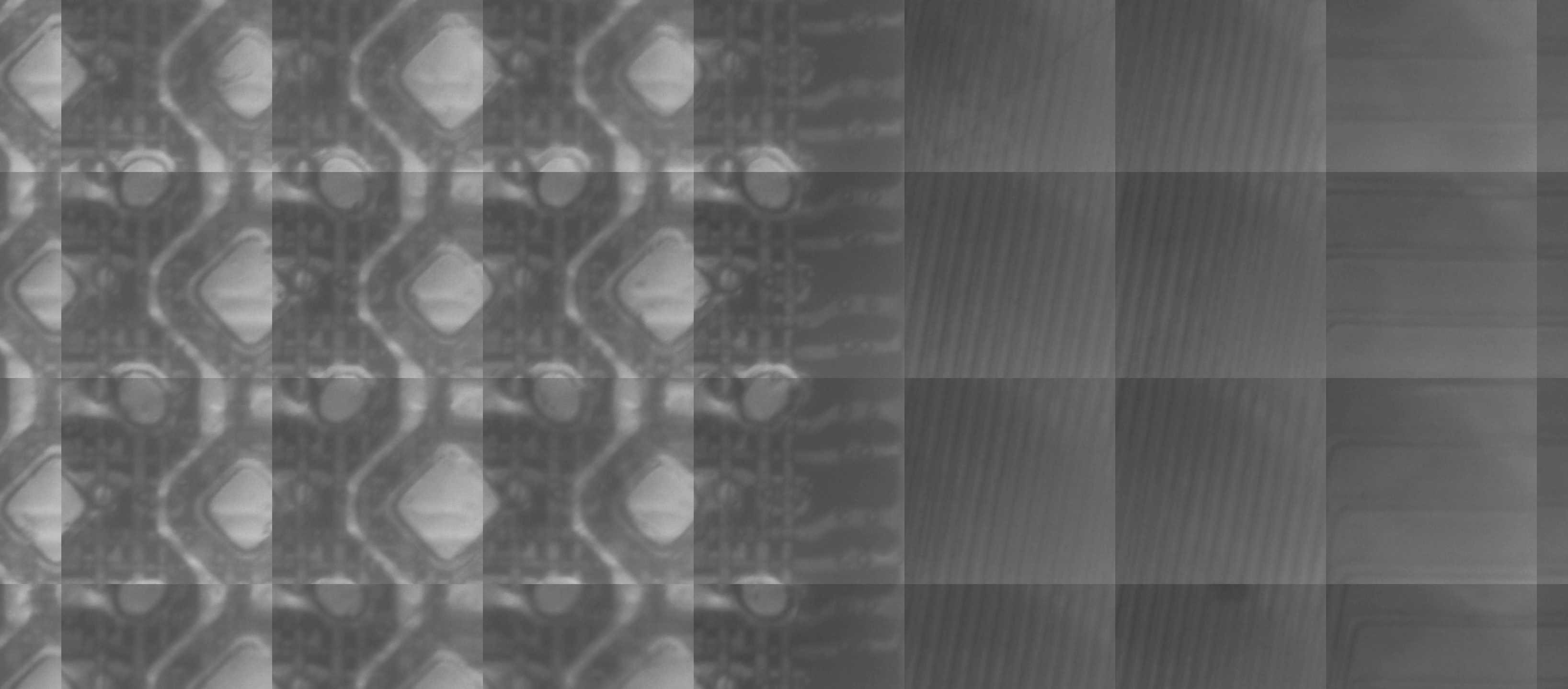
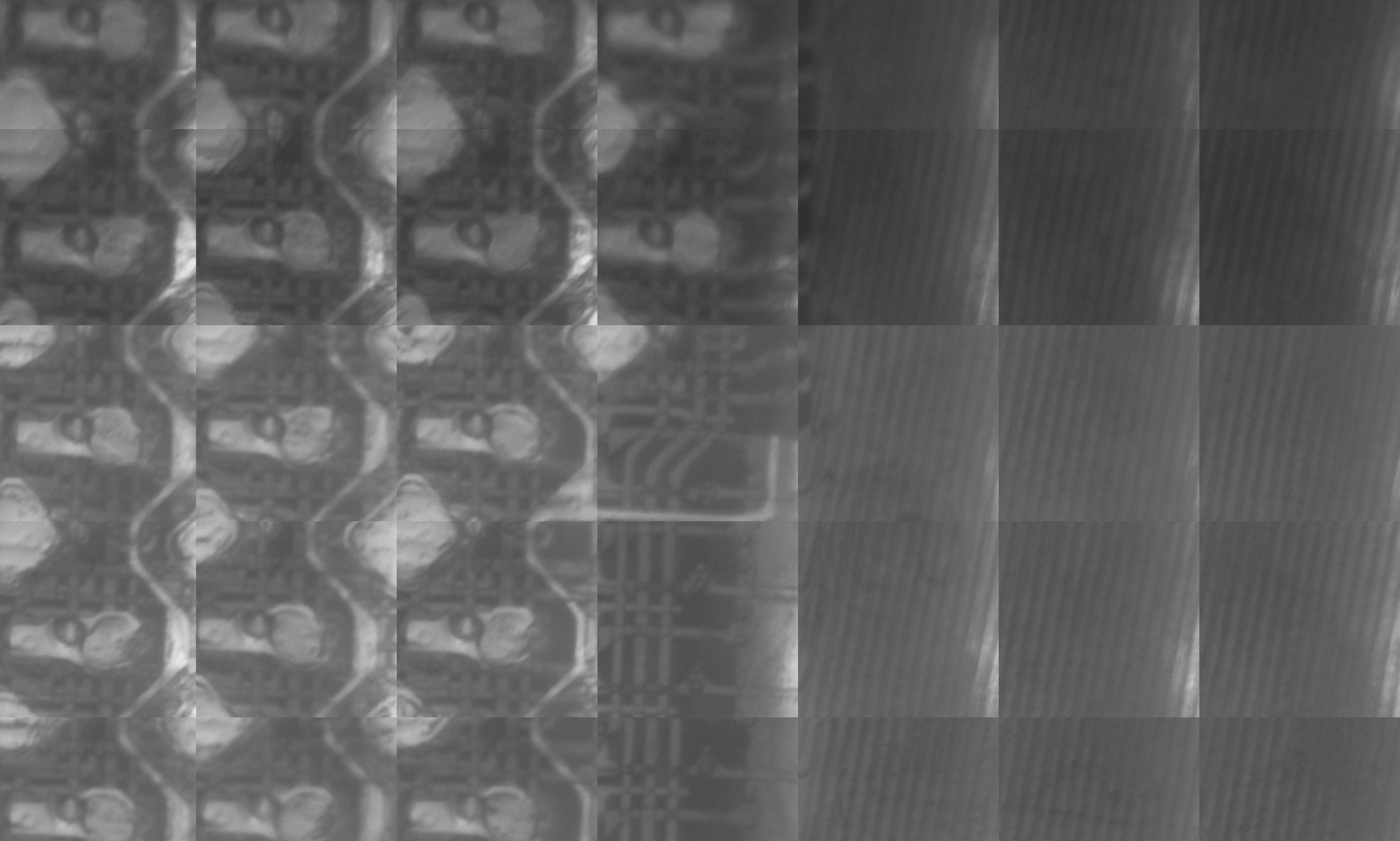
I was learning Python OpenCV for a couple mounth so I know I will capable of controll everything from python. I wrote a little code for move the X - Y movement like a scanner head, then I took pictures with the USB microscope and converted it to gray and added it them, so then I finally could take high resolution photos like below.
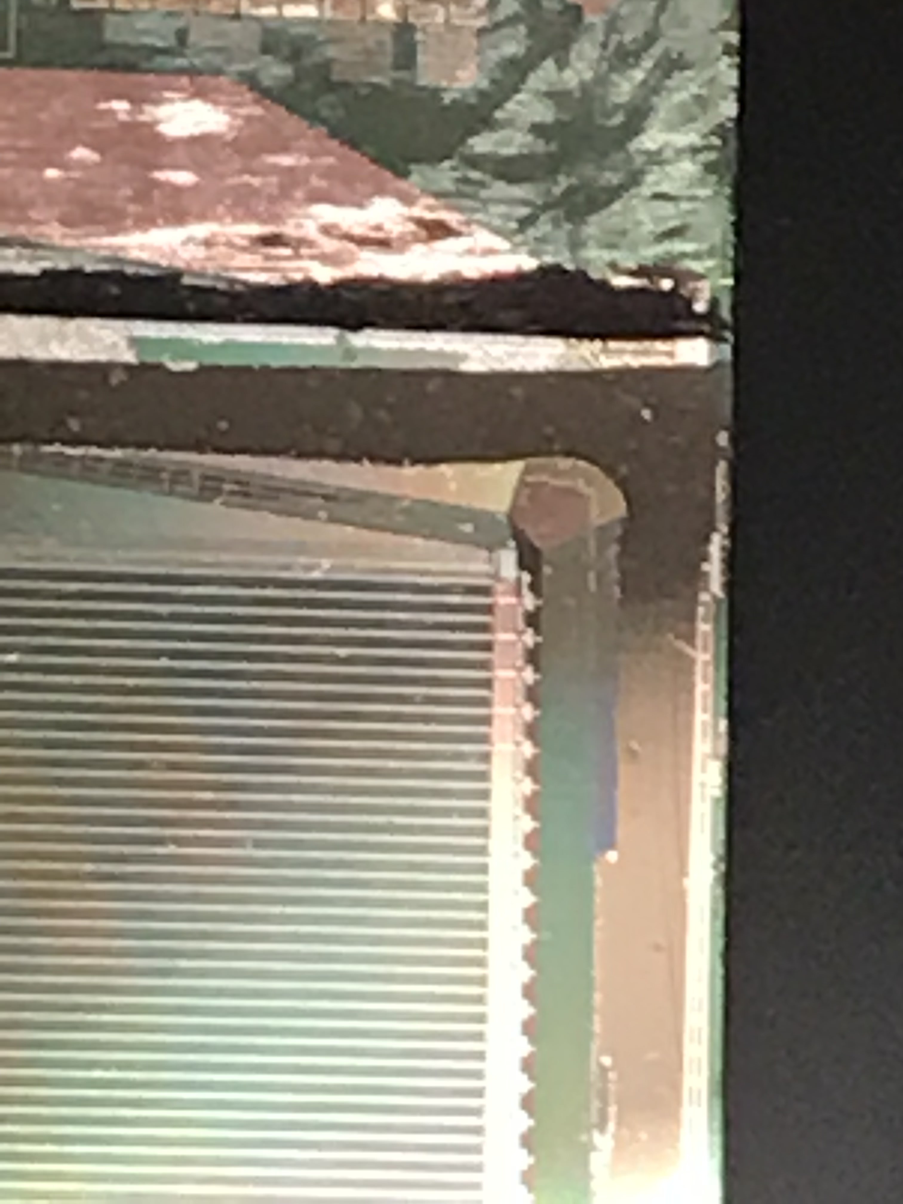
First show the display under 10X magnification from my Iphone camera, so you can compare how small these thing actually: (sorry for the bad focus, under this much magnification the phone could not focus very well)
And the scanned image under the microscope: (stiched together by python about ~200 picture)
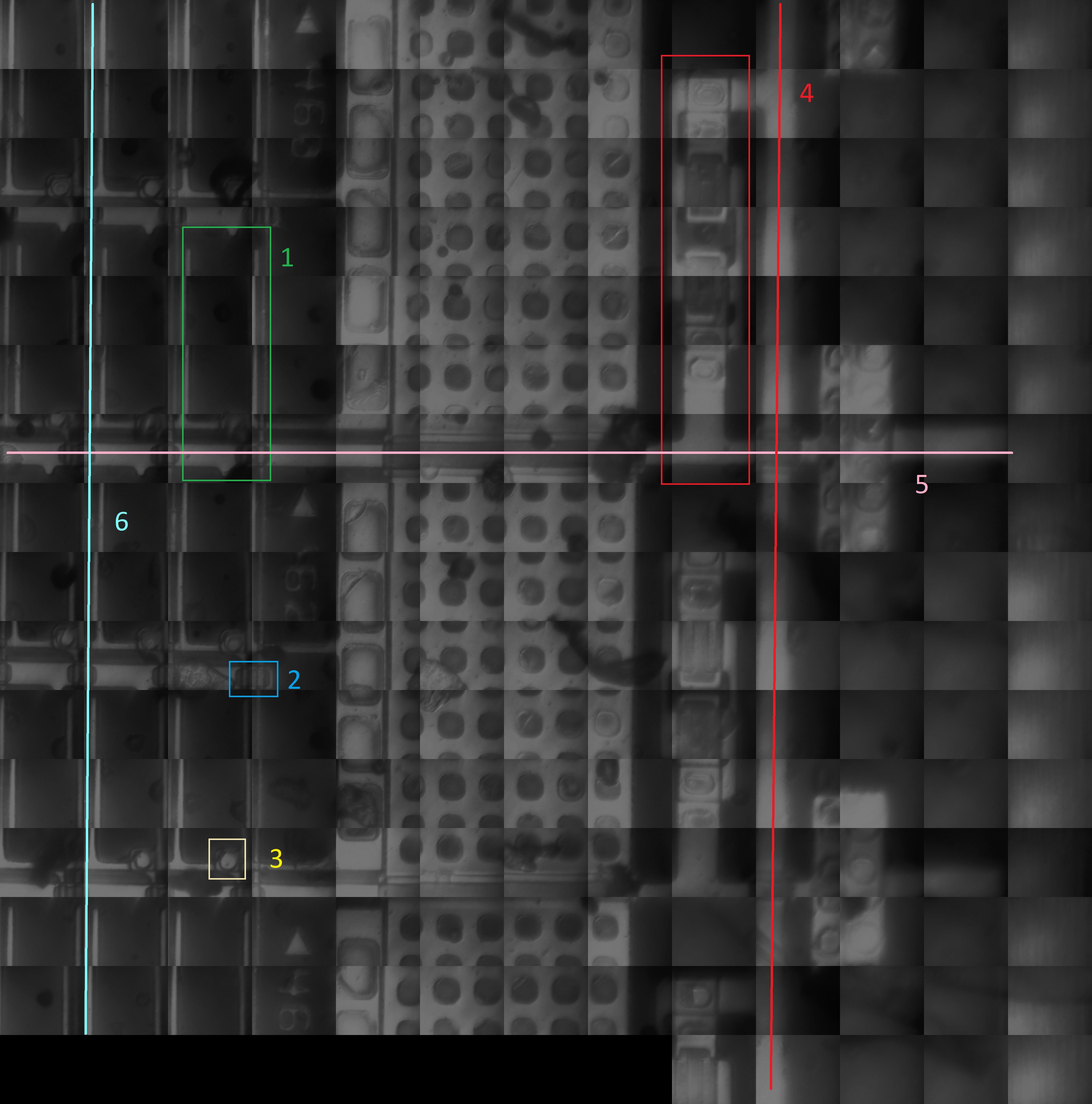
It is not so beautiful, but can be seen what needed. ...
Read more »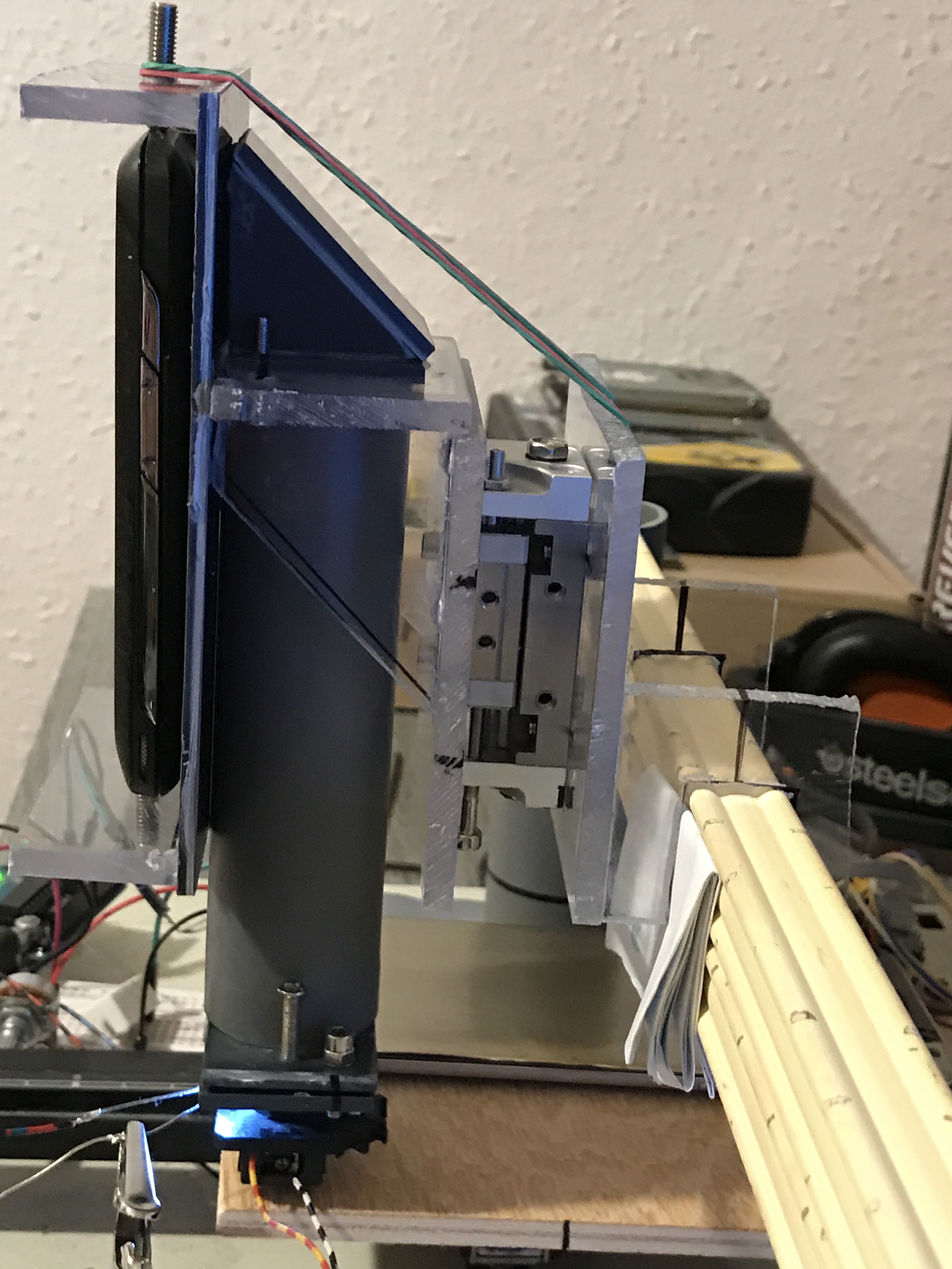


 Ahron Wayne
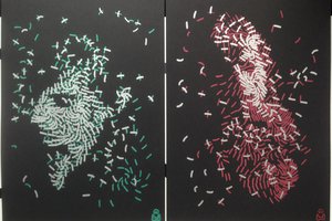
 Christian Walther
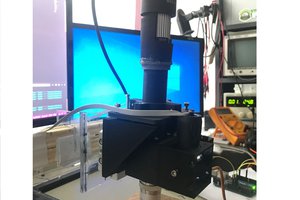
This is very cool. Thank you for documenting and sharing.
What are the lighter areas with the rows of 6 darker circles?