Microscope picture:
I asked a local mobile screen repair shop if they may have some damaged LCD or OLED screens for my research, and they said yes and gave me several Samsung S8 and S8+ Amoled screens for free. (Big thanks for the shop manager.)
As I found out these screens are really good and it looks like Samsung has way more experience over other display manufacturals that is insane. I choose the S8+ display to show, because the regular S8 screen has smaller pixels.
The S8+ display has the following parameters:
6.2" Quad HD+ Super AMOLED (2960x1440)
529 ppi
It is verry interresting under the microscope, it has a lot of details what I even could not see, because my home made microscope resolution was not good enough.
So lets see how the pixels looks like when they light up:
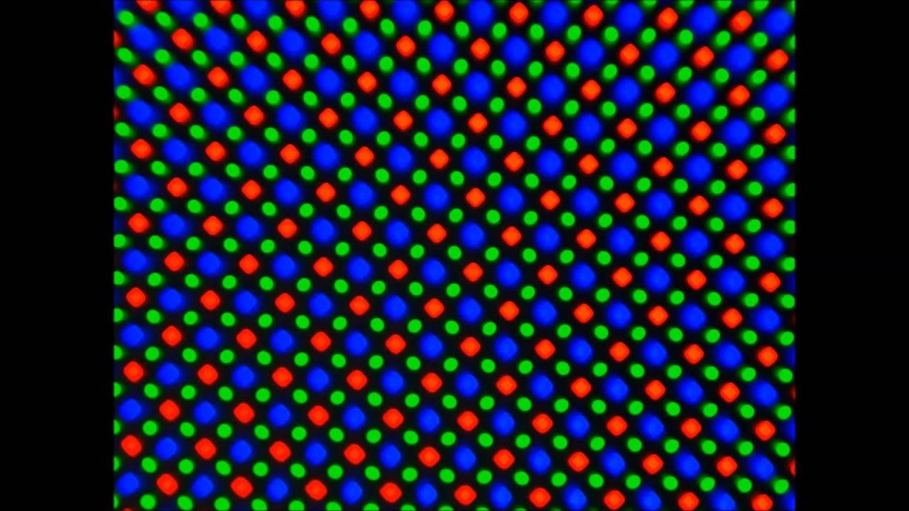
As you see Samsung used the Diamond pentile matrix. You see some color sub pixels are smaller or bigger. On LCD displays usually every pixel has 3 sub pixel, one RED one GREEN and one BLUE. In this case a full pixel has multiple sub pixels from each color, like one pixel has 4 green sub pixel.
I am not exactlly sure what is the benefits for this kind matrix, what if I have to guess these AMOLED screens hase much better color accuracy and the pixel will have much homogen light.
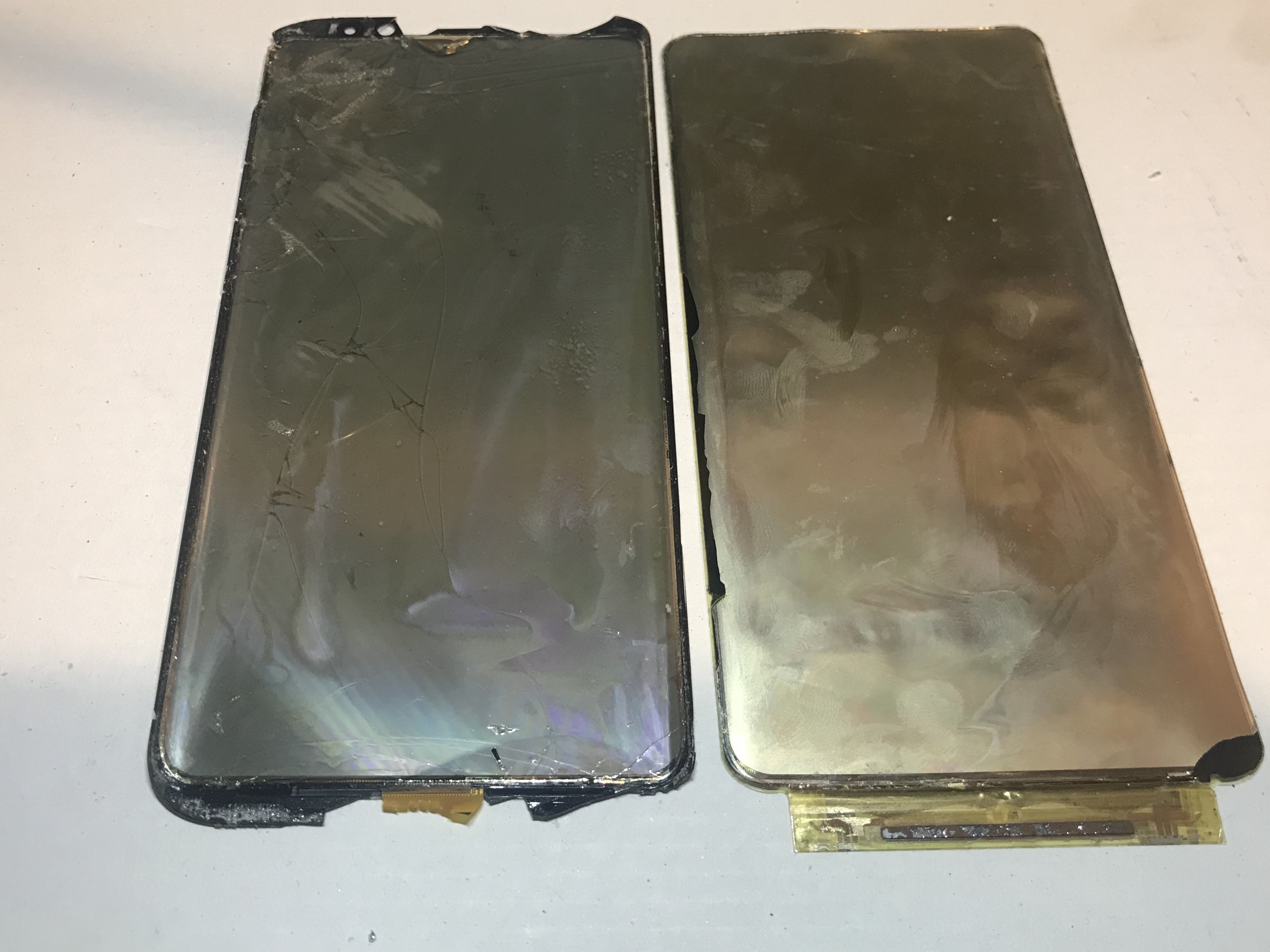
The sepatrated TFT+OLED layer from the front glass+touch layer:
Now lets see the screen under the microscope:
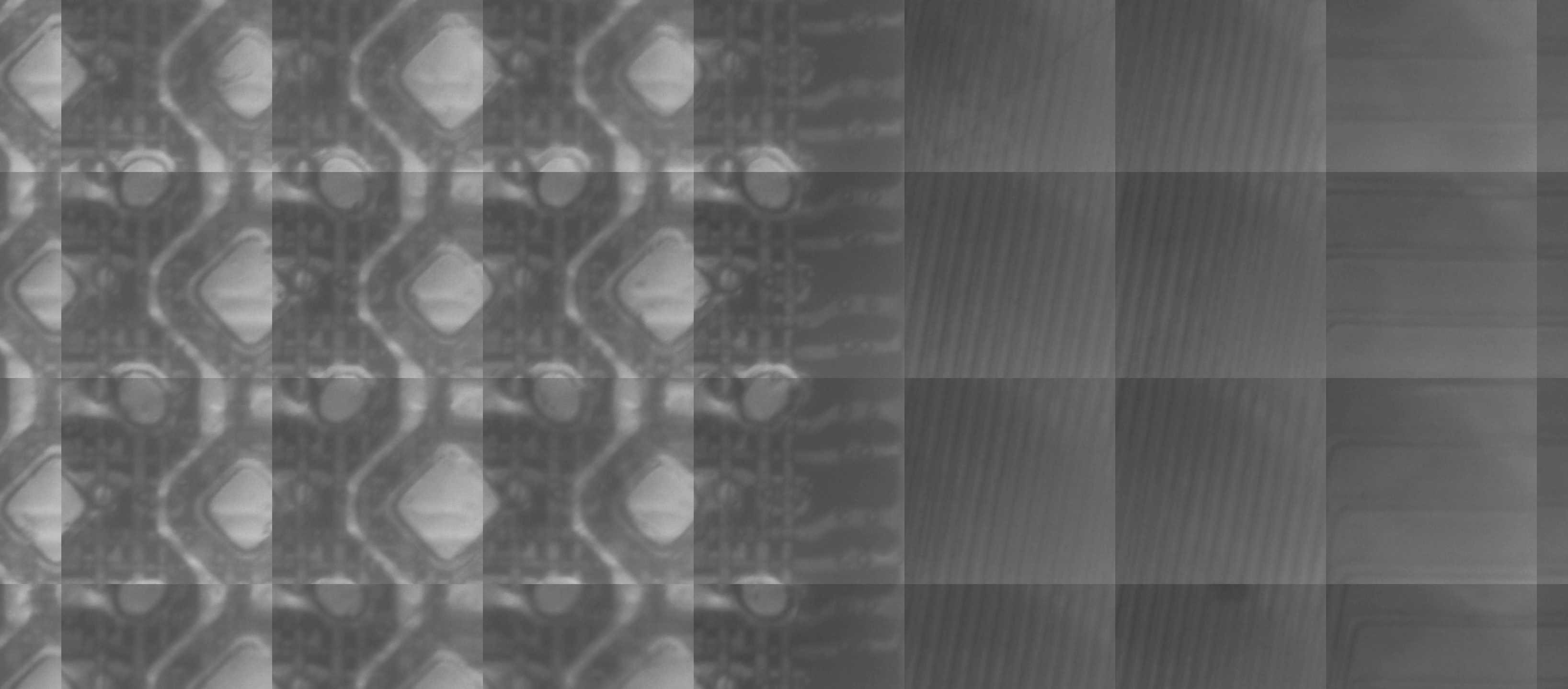
This picture was made from several little picture stiched togedher, each picture around 400 x 400 pixel, and the over all picture size is 5720 x 13760 pixel. The over all size is so large I could not upload it to this tread, only just to the download section, so if you are interrested in the full size pictures, please download them from the download section above.
Because of touch layer is top of the TFT and OLED layer I had to separate the two layer of the display, so it destroyed it, but it give us the main part what we came for.
The lines what you are seeing is the electrical trace which are controlling the sub pixels to light. The bigger rectangle is the BLUE sub pixel, the smaller rectangle is the RED subpixel. The GREEN pixel is quite different, it has a round shape.
The picture was taken from the bottom of the diplay edge, where the control lines leave the screen on the right.
The organic layer is sitting top of the TFT layer, so you actually can not see the TFT very clearly. If you are looking closely you will find some little round dots on the lines in the middle those are actually the transistors and active parts.
The Samsung displays has round edges on the corners, I made a little picture from it, when it is actually starting to "turn" round. You can see on the below picture, it is just missing one horizontal subpixel line from the middle and thats how it starts.
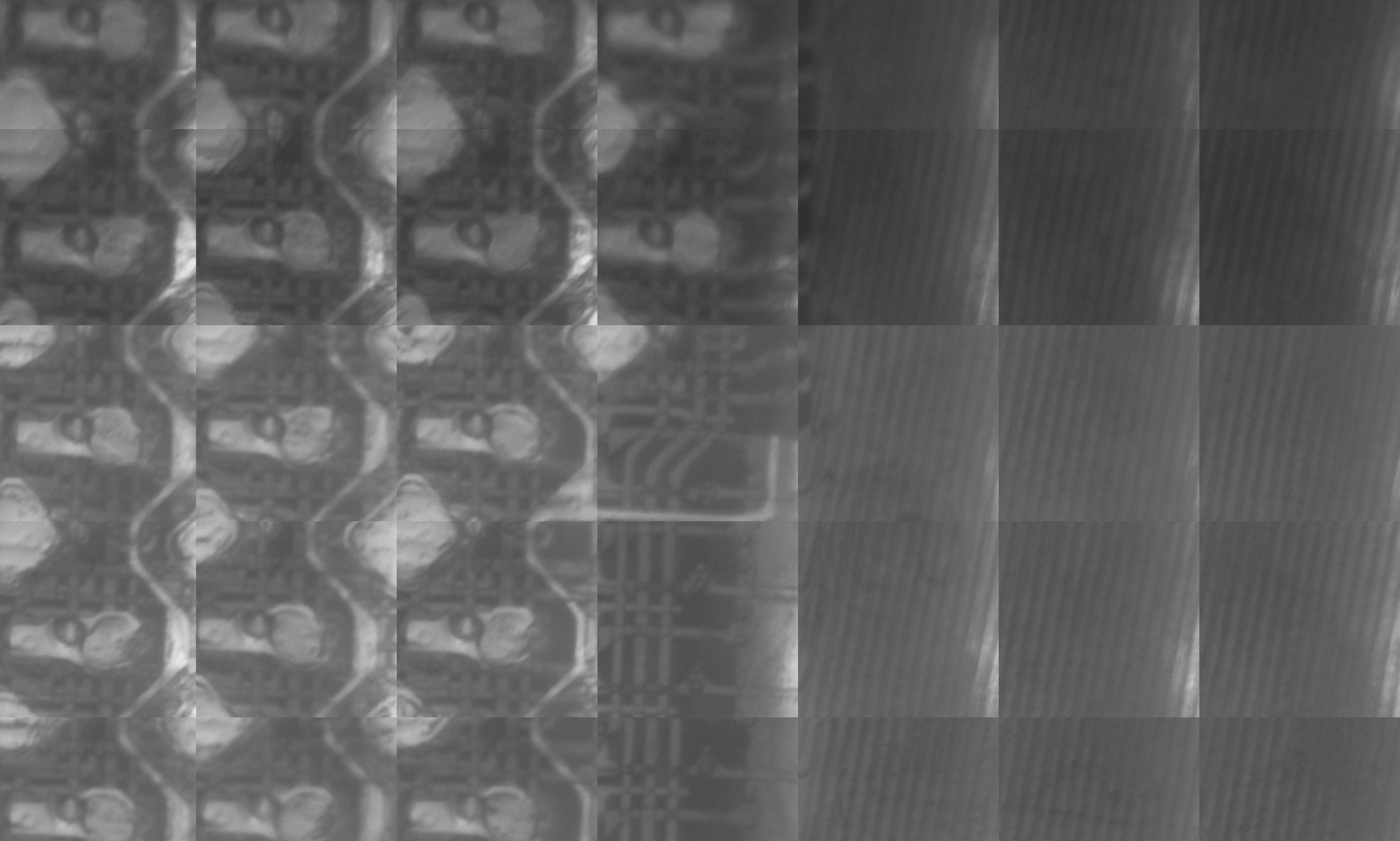
I am still working on the improvement of the picture quality, but it is not so easy anymore, because if you just calculate how big those lines on the pictures are, you will find out those are actually not bigger than 10-20um possibly it is closer to 10 microne, so pretty small.
I hope you find interresting this short article. Please go to the download section for the original size images.
Discussions
Become a Hackaday.io Member
Create an account to leave a comment. Already have an account? Log In.