 Jonathan Bumstead
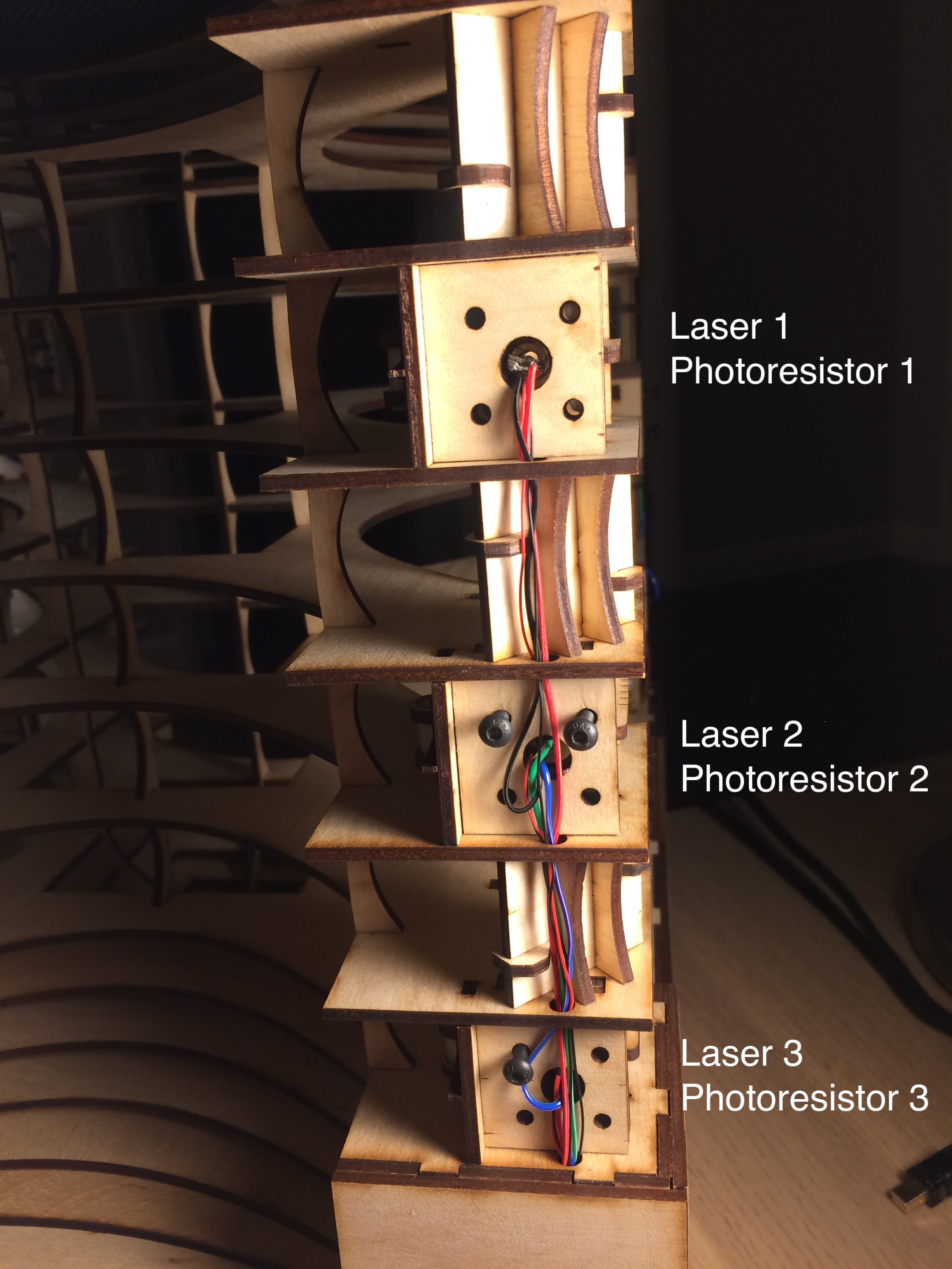
Each corner of the laser harp has three pairs of photoresistors and lasers. Therefore I need to run down the following signals to the electronics box:
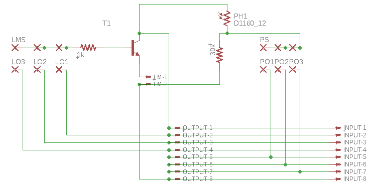
- Laser module control signal 1 (LO1)
- Laser module control signal 2 (LO2)
- Laser module control signal 3 (LO3)
- Photoresistor output 1 (PO1)
- Photoresistor output 2 (PO2)
- Photoresistor output 3 (PO3)
- Ground
- 5V
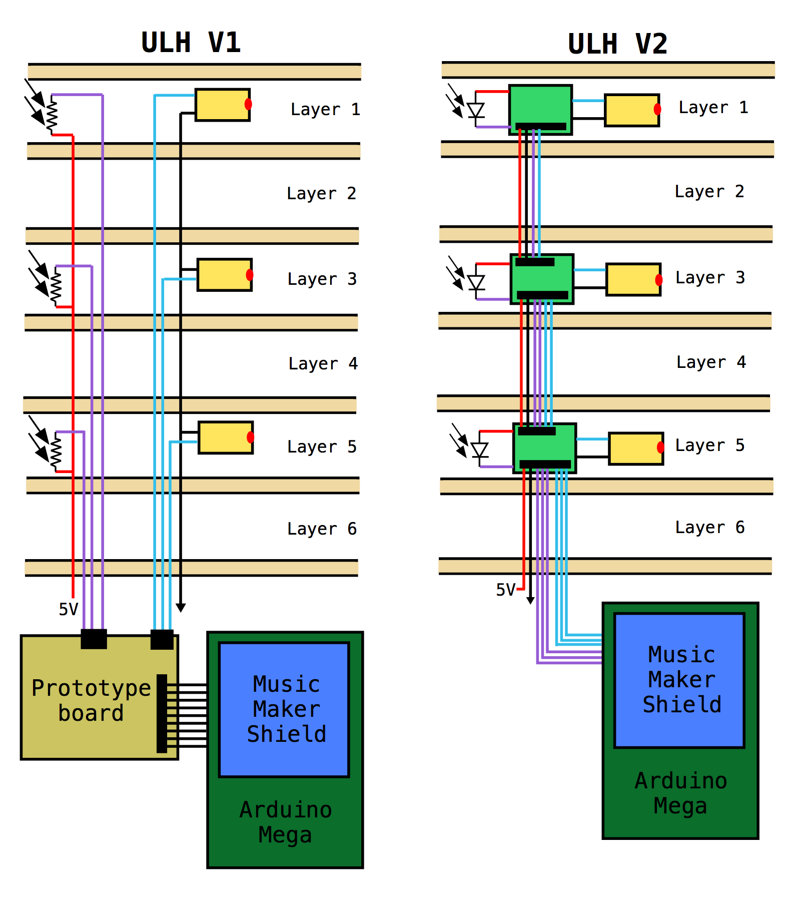
In the first prototype, the leads for the photoresistors and lasers were pulled down through each layer and connected to the control circuit in the electronics box. So the laser and photoresistors at the top required longer cables. This design makes it difficult to differentiate the control/output signals and manage the cables.
Instead of this strategy, I want to have a small PCB on each row for version 2. The PCB will include the electronics for generating the control signal and analog output that can connect directly into the Arduino. The output of each PCB would connect to the input of the next PCB on the way down to the electronics box.
I wanted to use the same PCB for each layer, so I needed a way to connect the control/output signals for each laser and photoresistor to the right pin. The solution was to add solder pads at the output of the laser/photoresistor and then three separate solder pads connected to the appropriate control pins. On each board, the laser output solder pad would then get shorted to the appropriate control signal pin. So for layer 1, the LMS node (control signal for the laser module) would get connected to LO1 (the first laser control signal). I designed the board in Autodesk Eagle with the help of my favorite tutorial by randofo on Instructables.
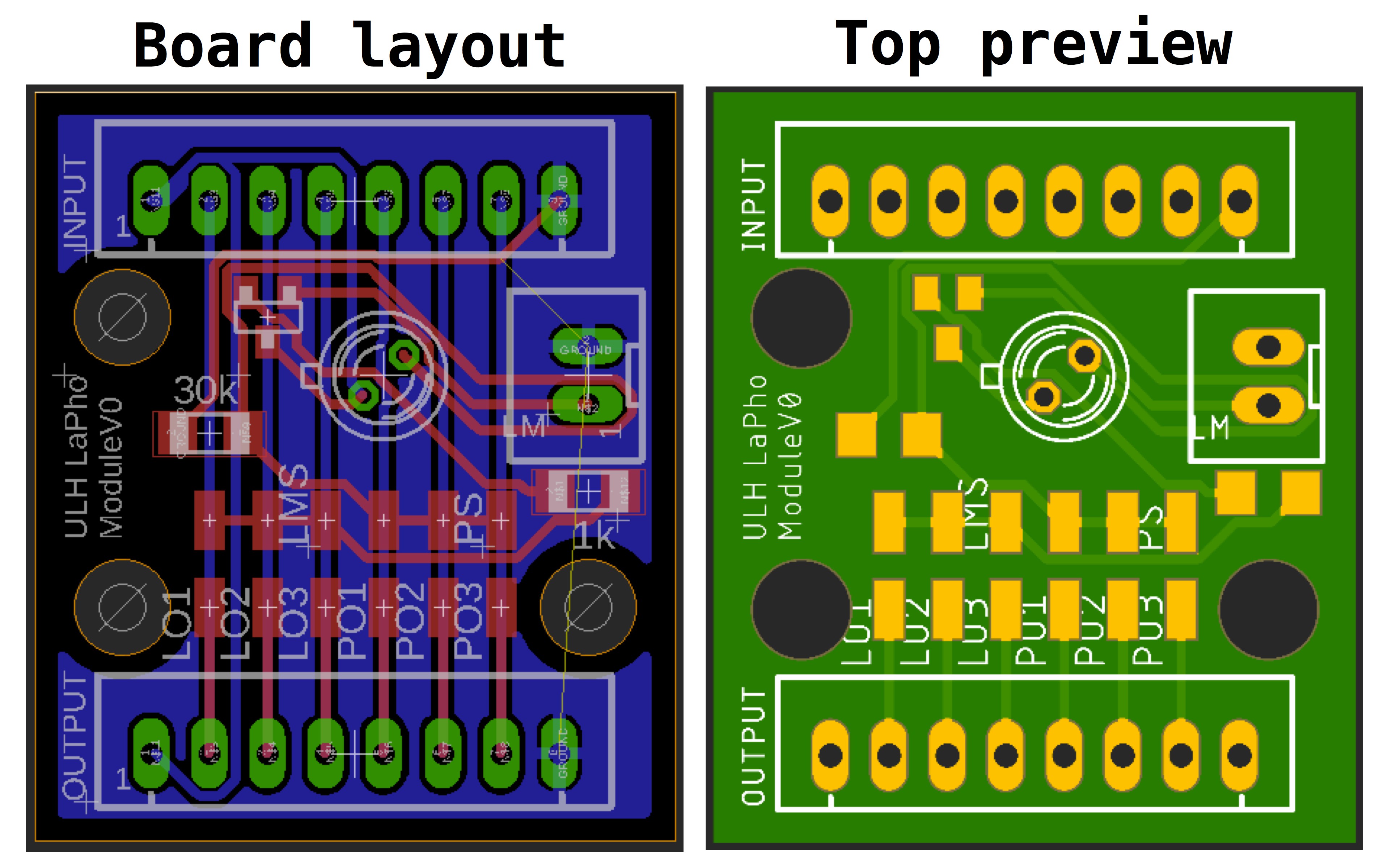
I'm happy with this board for the upright laser harp V2. Now I am onto importing the PCB into Fusion and integrating it with my new kinematic mount (which also needs a bit more work).
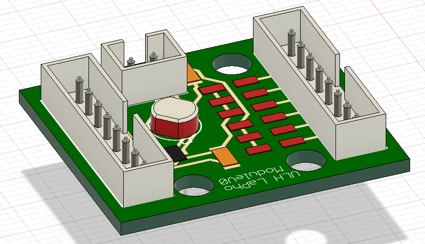
In the mechanical model, you can see the two 8-pin JST mounts for the input and output of the PCB (refer to the top of the log for the pin description). The board also has a 2-pin JST jack for the laser module. The only downside to this design is that I now need to accommodate larger 8-pin jacks running through each layer of the laser harp.
Discussions
Become a Hackaday.io Member
Create an account to leave a comment. Already have an account? Log In.