 Ted Yapo
An oscilloscope is for looking at waveforms, so I started digging around for some stuff to look at. I found the 74AUC gated ring oscillator I had discussed on another project, and fired it up. 74AUC logic outputs have interesting steps in their transitions because of their unique 3-stage output driver structure optimized for 50-65 Ohm transmission lines.
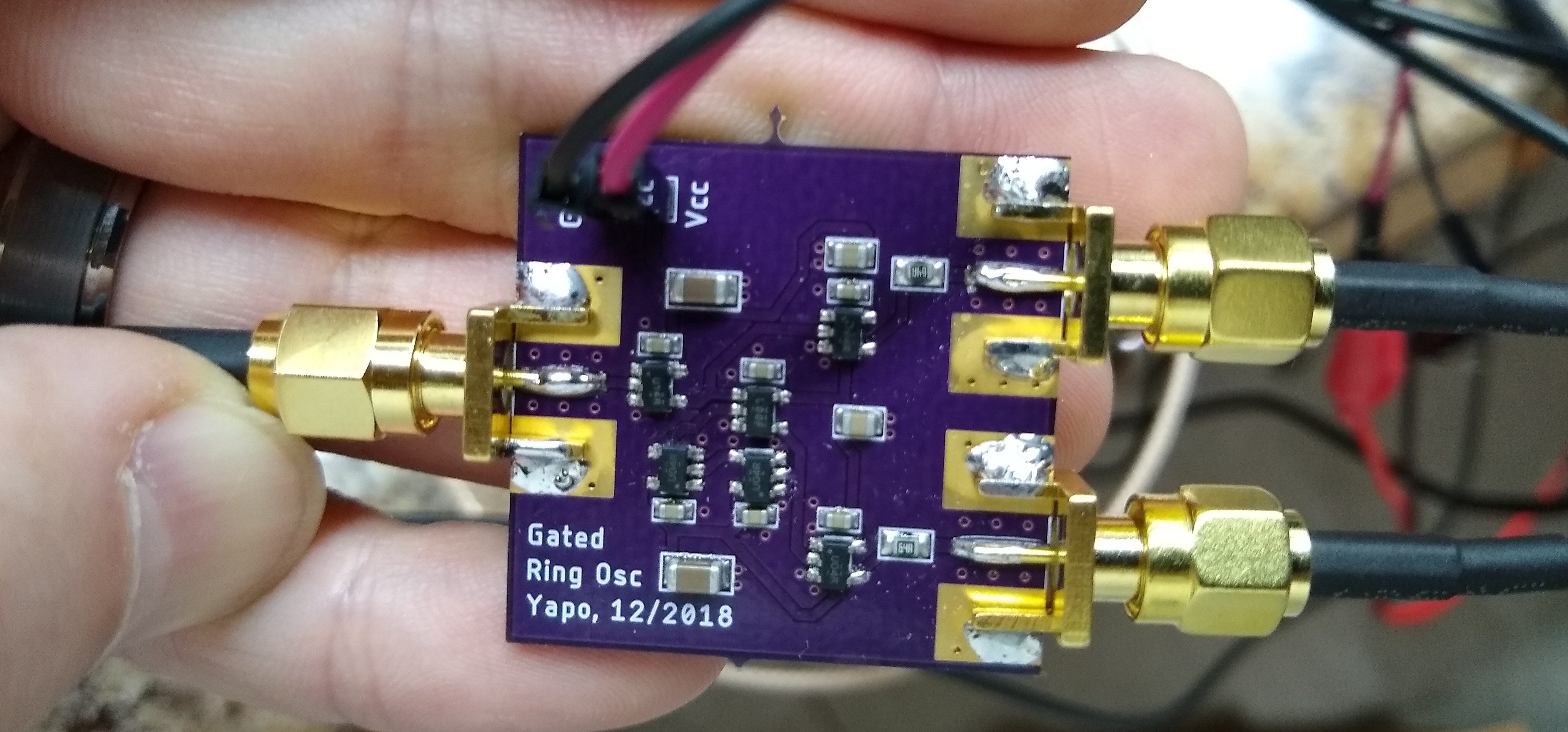
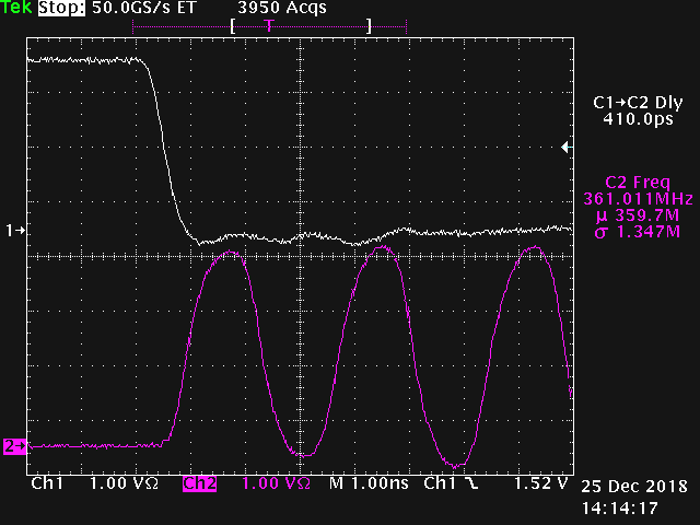
This oscillator, made with very-fast 74AUCxx gates, starts up quickly after the gate input transitions, and oscillates at around 360 MHz. Here is what the output looks like, just after startup, on the 20 GHz Tektronix scope and my prototype sampler of around 6.4 GHz:
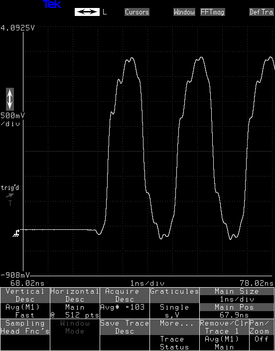
 You can see the three-stepped outputs on both scopes, although there is more detail in the left image from the Tek scope, but that's a 20 GHz instrument, so it's not really a fair comparison. Note that on a 1 GHz scope (image at end of log), you can't make out the steps at all.
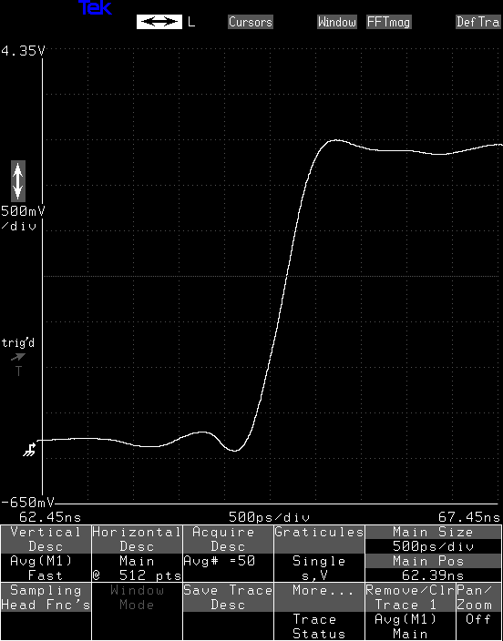
To get a more apples-to-apples comparison, I ran the Tek signal through a TL-11 delay line. This beast made to accompany the 11801 scope is a 47 ns analog delay line with a 70 ps rise time, which equates to a 5 GHz bandwidth. It's essentially a long, precision coax-cable-in-a-box. This should simulate what the signal would look like on a 5 GHz scope, or so I thought. Here's what you get:
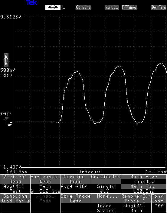
I can't explain the slow rising envelope at all. Ideally I would run the signal through the delay line for both scopes for the comparison, but I can't do that at the moment - the 47 ns delay messes up timing. But, in any case, some of the fine details are lost with this "5 GHz" simulated Tek scope, so it indicates that some of those details probably are above the 6.4 GHz 3dB cutoff of the prototype.
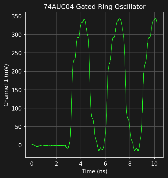
For reference, here's the waveform as I captured it on a slow 1 GHz oscilloscope back in December. With a 1 GHz scope, the finer details of the transitions are blurred, and you can't see evidence of the 3-stage output drivers at all.
Lol - check the date. That's what I was doing on Christmas day at two in the afternoon!
EDIT 20190827
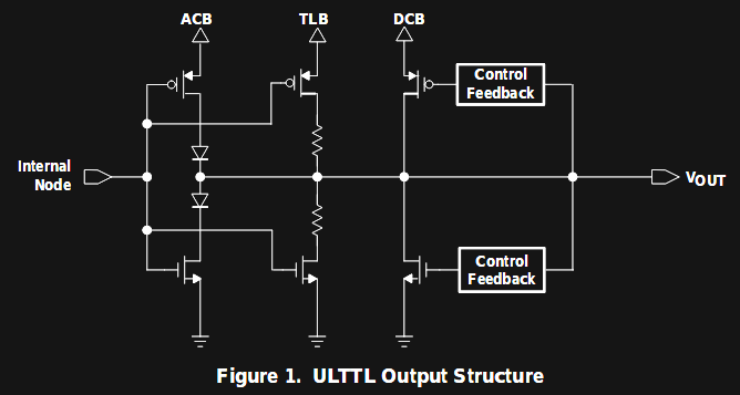
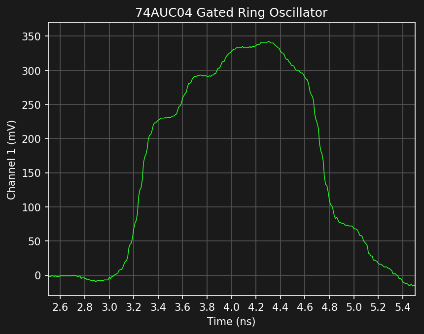
Here's the details of the 3-stage output driver in a 74AUCxx gate from TI's appnote, and a zoomed-in look at the stepped output waveform it produces. The steps are about 200 ps long.
At least, I think that's what you're seeing here. I need to put one of these gates on a PCB that just produces a step so I can see what happens later in the transition. Supposedly, the three stages switch over longer periods. Boards have been ordered.
UPDATE 20190828
I found another copy of the ring oscillator PCB and populated it with 74LVC parts. These are slower than the 74AUC, but have a traditional 2-transistor CMOS output structure. The transitions don't show the step artifacts, which points to them really being caused by the 3-stage outputs of the 74AUC gates rather than a reflection phenomenon on the PCB. Here are the Tektronix vs my sampler images:
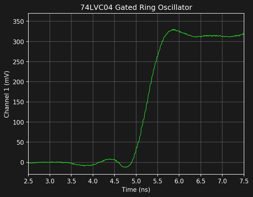
There is less noise in the Tek trace, but it also has been averaged 50 times. I could probably do better than I currently am.
But, I'm still not entirely convinced that I'm seeing artifacts from the 3-stage output drivers in the 74AUC parts. When the new boards come back, I should get a more definitive answer.
Discussions
Become a Hackaday.io Member
Create an account to leave a comment. Already have an account? Log In.