A major milestone reached today.
The Kobold K2, without debugger attached, runs a program from its two Flash ROM's, and blinks the LED on the main pcb !
It runs on the RC-clock that is on the main PCB (U9A, HC132, 4K7 and 470pF). No RAM has been mounted yet.
Here is the program:
; Kobold K2
; Blinking LED
; 20200125

start:
 nop
 movp 0,WP ; set wp and its page to zero
 movp 0x20,A2 ; address and page of output register

loop:

delay1:
 add 4,D0
 brnc delay1

 mov D1,(A2+28) ; led on

delay2:
 add 4,D0
 brnc delay2
 mov D1,(A2+30) ; led off
 jmp loop
Some notes about the program:
- The output is an addressable latch. Address bit A1 tells if the LED is on or off. So the value that is written to the address is unused, so there is no initializing of the D1 register needed. After a reset, this latch is reset and the LED is ON. So the LED is also a power indicator.
- The loop counter in D0 is never initialized. After adding 4 enough times, there will be a carry and the delay loop ends. At that moment, D0 has a low value again and can be used for the next delay loop.
- The WP (workspace pointer) is not used in the program, but it must be initialized otherwise the 8-bit immediate modes won't work.
- MOVP 0x20,A2 will set A2 to 0x0020, and it's page will be set to the lowest 4 bits of the 0x20 value, so it's page is set to zero. (Similar for WP that is set to zero).
It took about two weeks to reach this point. And of course, a job and other obligations limit the time that is available for the project.
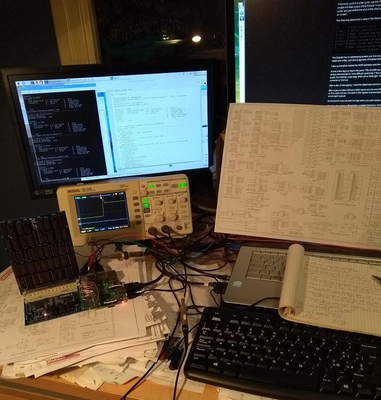
My desk during the debugging:
Just a summary of the things I encountered. This is mostly for myself, if I loose my notes then I can find here what I did. The notes start before the previous log, the numbers are the item numbers in my notebook.
1)
A problem with the clock generator on the main pcb. The Kobold needs two clock signals, on the main pcb these are called CPU_CLK/ and CLK2/. CPU_CLK/ must get active first, and stay active for 75% of the time. CLK2/ comes later, is active for 50%, and both clocks should end around the same moment. This phase relation was not correct. After the correction, CPU_CLK/ had a spike, that was removed with a small RC network. The final correction to the schematic was:
At pin 2 of U10A, a low-pass network 470E 33pF was inserted. U7B pin 11 was disconnected and connected to U7A pin 5.
3)
On the main board, one of the holes for the power connector was not big enough.
6)
Created S, I, M commands in the RPi script for debugging, see previous log.
7)
During debugging, the clock coming from GPIO8 is inverted wrt the CPU clock. This is not a problem, but if you don't know this, you get strange results.
8)
The HC299 did not put its contents on the bus (see previous log). Disconnected pin 1 and connected it to its pin 2 (on both devices). The shift-left function of the HC299 is now no longer available, but is now done by storing the register at any position in memory. This has as side-effect that the ALU adds the data register to itself and stores the result in the same register. And, surprisingly, the opcode doesn't even change. [edit: just found out the hard way, that the opcode does change. It is now the same as for a store instruction]
10)
Resistor R2 should get a more logical position on the pcb. Due to its strange position, I forgot to solder it.
12)
Started working on the Flash programmer. Starting point was the RPi Python script for the Risc Relay CPU. The RRC can only address words, while in the Kobold address bit A0 selects low or high byte, and is not connected to the Flash address bus. So the addresses had to shifted. Note that the RPi uses Kobold instructions to let the Kobold provide the correct address to the Flash. Both 8 bit Flash devices are programmed in parallel as if it were a single 16 bit wide device. The RPI provides the WE/ signal (on GPIO 25) to the flash to program it.
13)
The CE pulse from the RPI (Called DATA_EN/ on the main board) doesn't reach the Flash. It seems this can only reach the flash while the Kobold clock is active. (CE is needed to read from flash). First thing to check, before programmming, if the manufacturer and device ID can be read from the flash.
14)
Programming was working, but very unreliable. Problem was the 5V - 3V3 conversion. The connection board to the RPi has resistor dividers that bring 5V signals from Kobold down to 3V3 for the RPi. In the other direction, the 5V chips 'should' just accept 3V3 as high. In my previous projects, I used 5V powered HCT chips at those positions. Here I use HC and AC chips, and apparently did not think much about it.
In the end, I lowered voltage to the Kobold to 3V3. Both HC and AC can work at that voltage, and even programming the 5V Flash worked at 3V3. A final solution would be, to have a both-way voltage conversion to the RPi. To be done later.
15)
Problem with step-by-step executing from flash. It seems that the incremented PC is not written well to the HC760. Check if WE/ (U36 pin10) goes high before SHFT_OE/ (U26 pin 1,2,3) goes high. The difference is difficult to measure, seems to be less than 3 nS. This was anticipated as possible problem. C50 was not mounted yet, now mounted 120pF that gave about 10nS margin, looks enough.
Also, a problem was found with the reset. But this can be solved later, because for now, the CPU can be reset by giving commands from the RPI (instructions to reset PC and its page to zero).
16)
Now I had a strange problem, when executing commands from the debugger. Sometimes, bit 5 got set in the data. After trying several combinations, I got it reproducable. It occured when the WP and its page were initialized to zero. The instruction is "MOVP 0,WP" and it is assembled as opcode 211E. This is 16-bit immediate mode. It assumes the programcounter points at the beginning of a 32-byte chunk, and the LSB of the instruction tells that the immediate value can be found at PC+0x1E (the last address of the chunk).
When entering the instructions from the debugger, just enter "I 211E" and then the operand "M 0000". Never mind the value of the PC. The Kobold won't mind that the operand doesn't come from memory.... BUT... The programcounter does have a certain value, and when the 0x1E is added by the adder chip U32, there will be a carry when the PC is not zero... This carry goes to the OR chip U42C to bit 5 of the adder chip U6 of the ALU... causing 0x20 to be added to the data ! That is the way it is designed. It is used for adding a small constant to an address register. When the small adder U32 overflows, the carry is handled by the main ALU.
So when you don't know the PC value during debugging, use "2100" for loading the WP, that will add 0 in the U32 adder and will never generate a carry there.
If you have a strange architecture, beware that you will have strange results during debugging...
Another one in the same category: Some instructions contain an 8-bit immediate operand directly in the instruction. Moving the value 0x34 to register D0 has code "7C34". So we enter the instruction with the I command, and for the execute cycle we just enter "M 0", knowing that this data is not used, because the processor already has the 0x34 value. Wrong. It just loads zero instead of the expected 0x34.
The "M"command disables outputs from Kobold or Memory, so the RPi can put that value on the bus. But in Immediate 8-bit mode, the Kobold first places the immediate data on the databus with the buffer unit, and then the ALU reads that data as if it was coming from memory ! The M command disables the buffer unit, so the "M 0" zero is going to the ALU ! So use the W command instead, that generates an execute-clock-pulse but lets the Kobold or memory drive the databus.
18)
The problem with the reset, mentioned earlier, is solved with a hardware modification. The reset connects to the instruction register (setting it to zero) and to the shift unit (setting it to zero). So at reset, it will execute an instruction with opcode "0000", that will write a value to the PC and to the page of the PC. Resetting the shift unit makes that the written value is zero. BUT... we have no control over the moment that the reset pulse ends. When it ends, the shift unit will at the following clock be filled with some value from the ALU, while the instruction register still has the instruction to send that value to the PC. So, a probably non-zero value, coming from the ALU, will be put in the PC.
It was solved by driving the reset of the shift unit also from the instruction register, by decoding sufficient bits of the "0000" instruction:
Decoder U44B is now used (was unused). Its input pin 15 connects to pin 4 of U44A, and its input pin 14 connects to pin 15 of U43. Its output at pin 12 now connects to the CLR inputs of U25 and U26 (pins 9).
999)
Well that was a not-too-short list of challenges that I encountered before I got the LEDs blinking.
Now I have a Blinking LED..... yes I could also do that with a 555...
Discussions
Become a Hackaday.io Member
Create an account to leave a comment. Already have an account? Log In.