 land-boards.com
Thinking through the PSoC design and how to implement peripherals. Want:
- Mailbox with status register (read/write ready)
- I/O Address Latch
- 8-bit Data Read/Write register
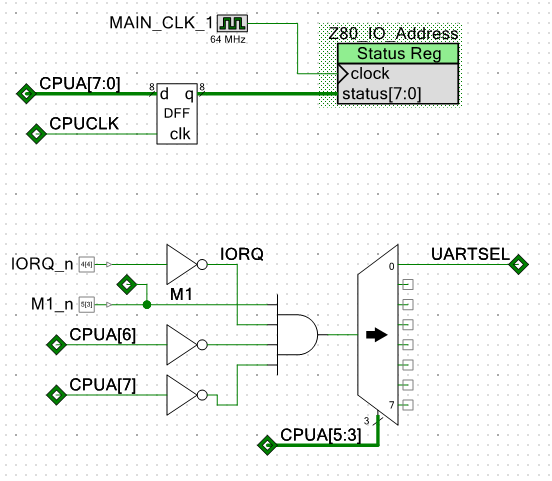
Z80 I/O Address Latch in PSoC
Latches the 8-bits of address from the Z80. This address can be read by the PSoC via the Z80_IO_Address Status Register.
I/O Chip Selects can be hard decoded.
I/O Mailbox
The I/O mailbox circuit is implemented with data and control/status register as follows:
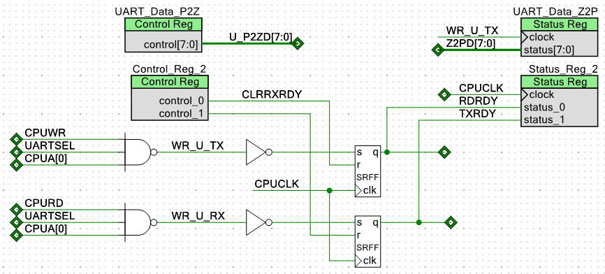
The PSoC writes to the UART_Data_P2Z register which can be read from the Z80. RS Flip Flops are set when the UART_Data_P2Z is written from the Z80 or UART_Data_Z2P is read by the Z80. Bits from the Control_Reg_2 is used to clear the RS Flip Flops. Status_Reg_2 is used to read the output of the RS Flip Flops by (or can cause interrupts to) the PSoC.
Discussions
Become a Hackaday.io Member
Create an account to leave a comment. Already have an account? Log In.