 land-boards.com
There is only one device in the memory space, a 512KB SRAM. The Z80 only supports 16-bits of address. This function does bank switching and mapping.
There are software builds for the Z80 which have ROM and RAM. The RAM is typically copied to the RAM and then the program is run out of RAM. CP/M builds use this method. Part of this was that the EPROMs of the day were relatively slow compared to RAM. Today, RAM is very fast. Maybe too fast.
Switching between the banks varies by the hardware implementation and software needs. The PSoC can go a low way towards this functionality by performing banking control. This circuit is a first cut at that.
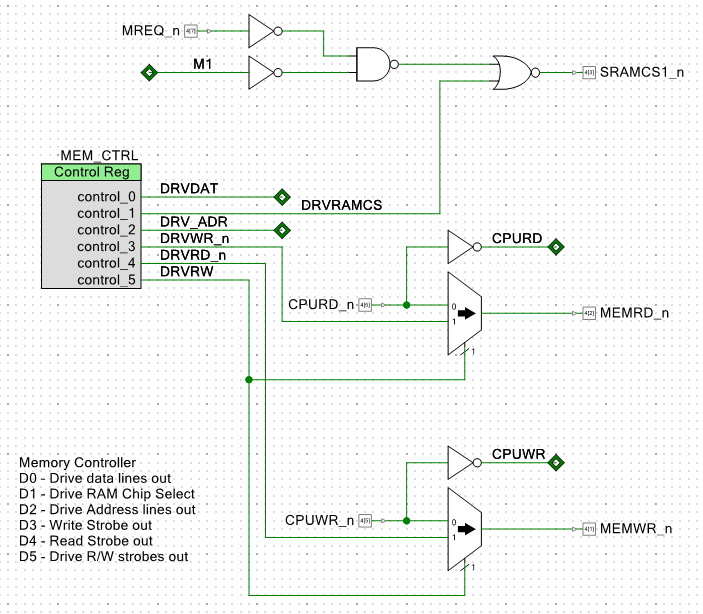
Chip Selects and Read/Write Strobes
Banking
Banking consists of re-mapping some of the upper bits of the Z80 address bus into more address bits of the SRAM. This could be done purely in hardware with a small mapping function (like a RAM) or with the help of the PSoC. This means the PSoC writes to the BANK_REG with the upper SRAM address lines. For this implementation I've chosen to bank switch address lists 13..15. This provides for 8 banks. These three bits map to SRAM 13..18 address lines.
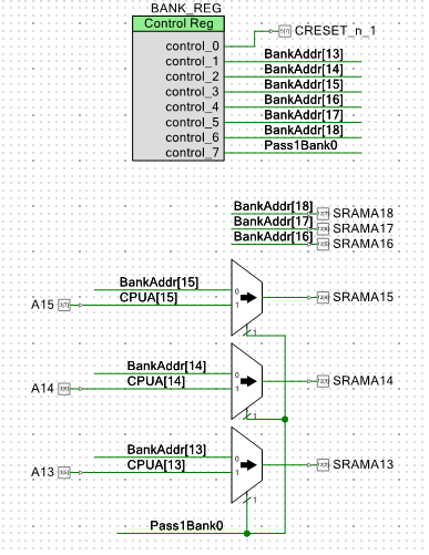
There will probably need to be some more registers for mapping but this logic provides a "direct" path where the CPU addresses go directly through (all 64KB are directly mapped) and the ability to swap in upper bits from the bank register values.
The I/O select logic (previous page) indicates to the PSoC that a bank select operation needs to be done.
Discussions
Become a Hackaday.io Member
Create an account to leave a comment. Already have an account? Log In.