 land-boards.com
The performance should closely match the original designs.
CPU Performance
The program memory needs to be able to keep up with the CPU. The CPU should be able to run with no wait states. Let's verify the timing works.
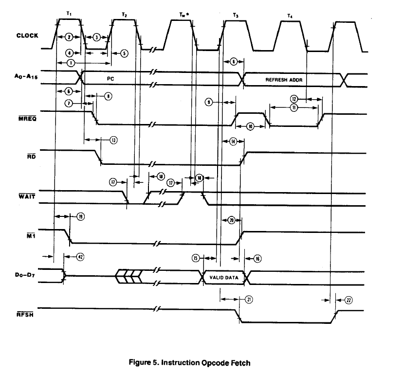
Opcode Fetches
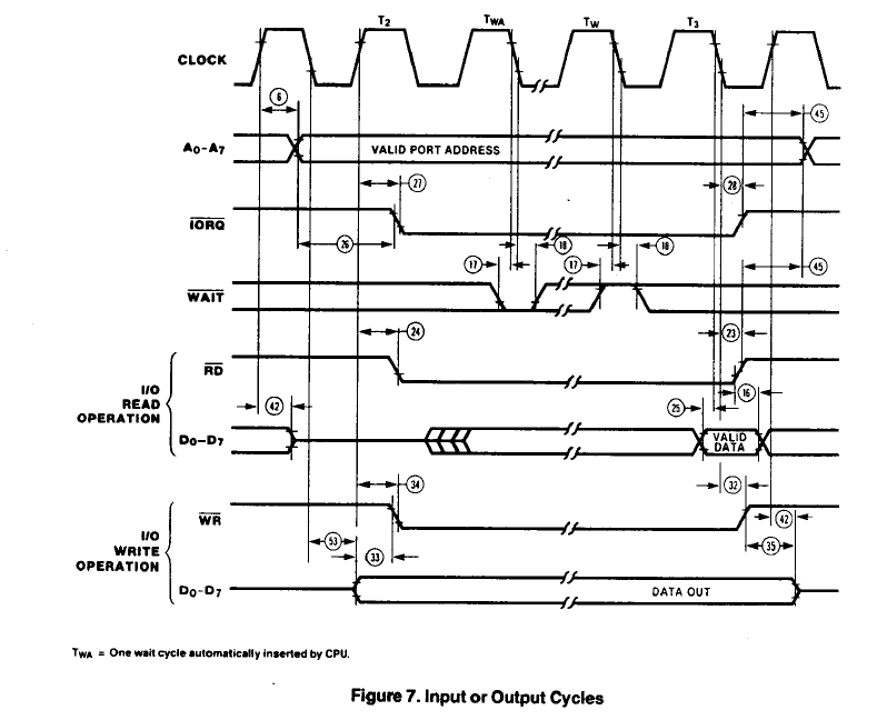
Opcode fetches take four clocks on the Z80 (plus any wait states). The CPU is run at 8 MHz (could easily be pretty much any available speed) The RD* strobe is approx 1-1/2 clocks wide. With a 6 MHz CPU (166 nS clock rate) this is 249 nS. MREQ* drops 80 nS max (13) after the clock falling edge. Data is read on the rising edge of T3 and has a required setup time of 30 nS min (15). The address is guaranteed to be valid 35 nS before MREQ* falls.
The SRAM access speed is specified from address being valid. The address is valid 90 nS max (6) from the rising edge of T1. It is also guaranteed to be valid prior to MREQ* falling by 35 nS (min).
Timing would then be the 249 nS minus 80 minus 30. If the SRAM is faster than 139 nS it will run with no wait states. The SRAM I selected is 55 nS so it is more than fast enough to read instructions without wait states.
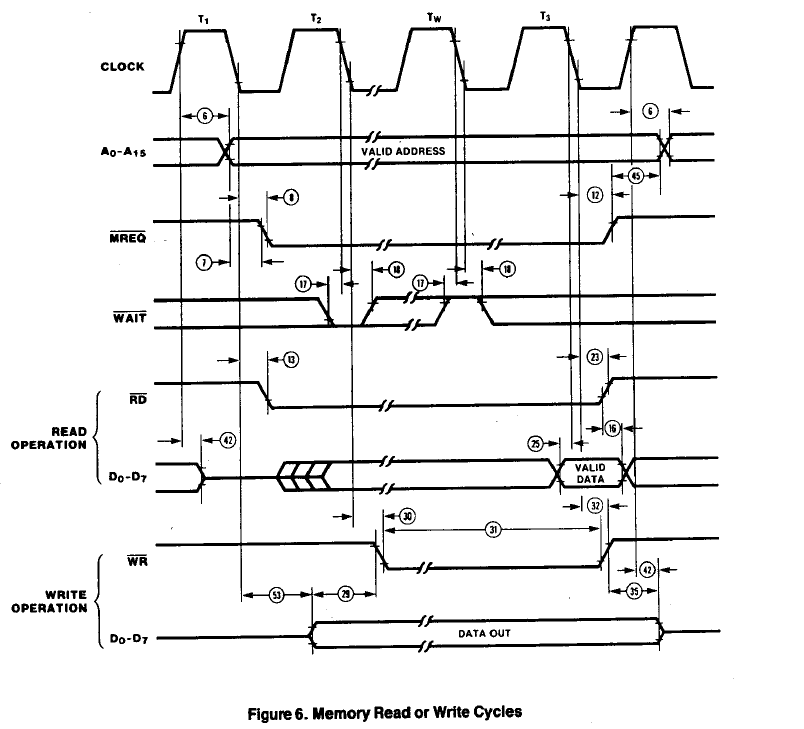
Data Reads/Writes from/to SRAM
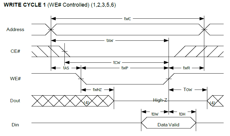
Data read timing is identical to opcode read timing so there's no issue for speed. Writes are set by the width of the WR* pulse. This is 132 nS (31). This also is fast enough. Fortunately the data hold time after RD* rise is 0 nS (16).
SRAM Timing
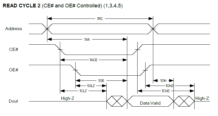
The SRAM timing shows that the output enable to output is very quick.
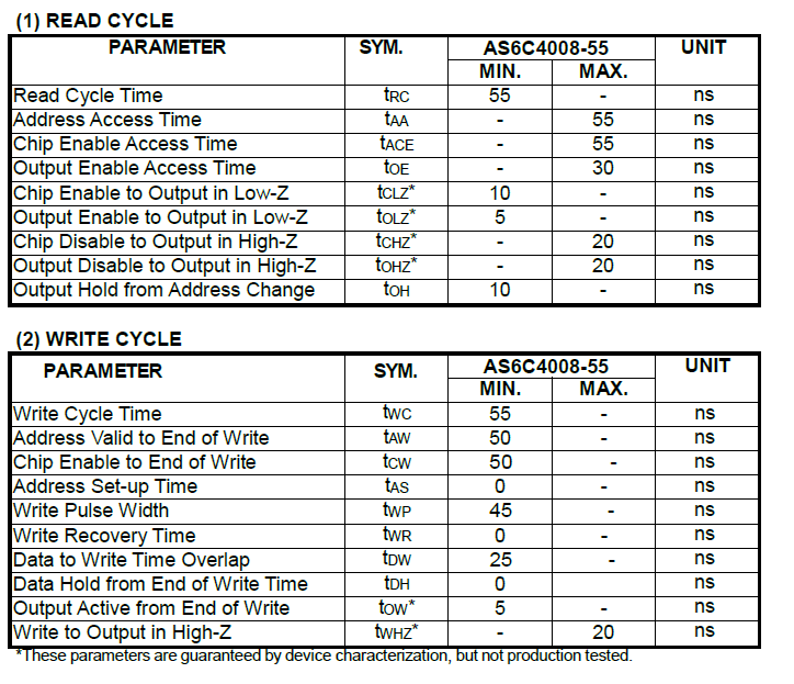
Read Cycle timing is:
Write cycle timing is:
I/O Performance
The only speed exception could possibly be reading of peripheral devices (and writing of some devices). That is because the devices are essentially emulated by the PSoC. I/O may need to assert wait states.
Discussions
Become a Hackaday.io Member
Create an account to leave a comment. Already have an account? Log In.